Hybrid PVD-CVD system

a technology of hybrid pvd and cvd, applied in the direction of vacuum evaporation coating, chemical vapor deposition coating, coating, etc., can solve the problems of not being economically or technically capable to be coupled together in a single processing system, the number of substrate transfer between different tools has an adverse effect on product yield and throughput, and the number of substrate transfer between different tools is high

Inactive Publication Date: 2007-01-25
APPLIED MATERIALS INC
View PDF4 Cites 102 Cited by
  • Summary
  • Abstract
  • Description
  • Claims
  • Application Information

AI Technical Summary

Benefits of technology

[0012] In another embodiment, a method of processing a substrate includes loading the substrate into a first load lock chamber of a substrate processing system, transferring the substrate from the first load lock chamber through a first transfer chamber into a second transfer chamber, and transferring the substrate into one or more chemical vapor deposition chambers of the substrate processing system. The method further includes depositing one or more silicon-containing layers on the substrate by the one or more chemical vapor deposition chambers of the substrate processing system, transferring the substrate from the one or more chemical vapor deposition chambers into the second transfer chamber, transferring the substrate from the second transfer chamber into the first transfer chamber, and transferring the substrate form the second transfer chamber into one or more physical vapor chambers of the same substrate processing system without breaking any vacuum. Further, the method includes depositing one or more metal-containing layers on the surface of the one or more silicon-containing layers by the one or more physical vapor chambers, transferring the substrate from the one or more physical vapor deposition chambers into the first load lock chamber, and unloading the substrate from the first load lock chamber of the substrate processing system.
[0013] In addition, a substrate processing system for processing one or more substrates is provided. The substrate processing system includes one or more load lock chambers, one or more transfer chambers coupled to the one or more load lock chambers, and one or more chemical vapor deposition chambers coupled to the one or more transfer chambers and configured to deposit one or more silicon-containing layers on the substrate. The substrate processing system further includes one or more physical vapor deposition chambers coupled to the one or more transfer chambers and configured to deposit one or more metal-containing layers on the substrate.
[0014] In another embodiment, a substrate processing system for processing one or more substrates includes a first load lock chamber for loading and unloading the one or more substrates, a first transfer chamber coupled to the first load lock chamber, and a first process module coupled to the first transfer chamber. The substrate processing system further includes a second process module coupled to the first transfer chamber via a second load lock chamber. The first process module includes one or more first process chambers and the second process module includes one or more second process chambers configured to perform a different process than the one

Problems solved by technology

Another reason is that different types of films generally require different types of process chambers and chamber peripherals that may not be technically capable or economical to be coupled together in a single processing system.
Since the surface of a silicon-containing film tends to be oxidized when exposed to air so the deposited silicon-containing film needs to be cleaned and/or processed immediately within certain time frame due to the increase potential for particle contamination, moisture penetration, and surface oxidation before and/or after a next patterning step or deposition

Method used


Image

  • Hybrid PVD-CVD system
  • Hybrid PVD-CVD system
  • Hybrid PVD-CVD system

Examples


Embodiment Construction

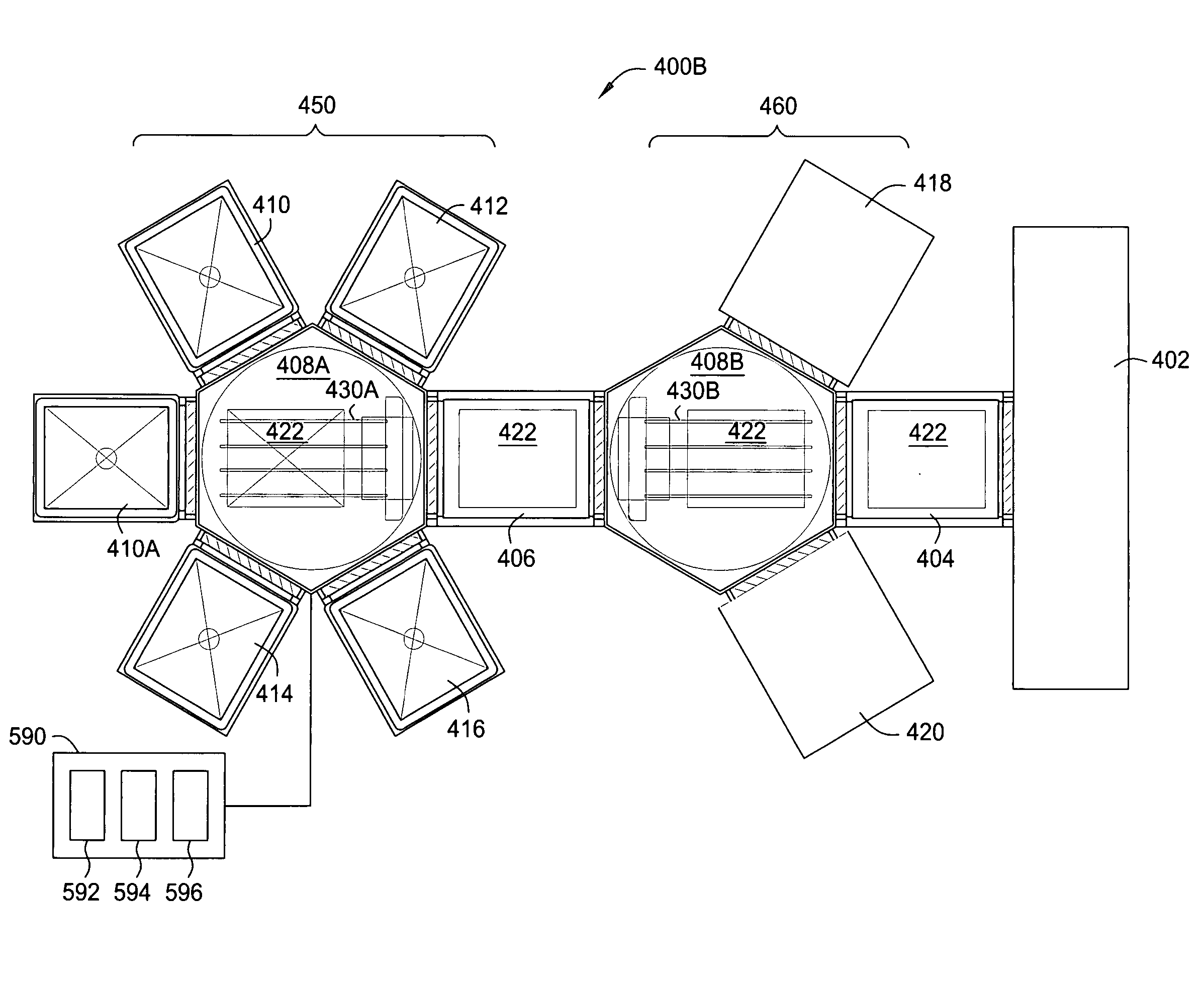
[0045] The invention provides a method and a substrate processing system for in-situ processing of a film stack containing one or more silicon-containing layers and one or more metal layers without taking the substrate out of the substrate processing system or cleaning the substrate in between the silicon-containing and / or metal layers are deposited. The silicon-containing layers and the metal containing layers can be processed in high volume and high throughput by different types of process chambers, for example, physical vapor deposition (PVD) and sputtering chambers, ion metal implant (IMP) chambers, chemical vapor deposition (CVD) chambers, atomic layer deposition (ALD) chambers, plasma etching chambers, annealing chambers, other furnace chambers, cleaning stations, etc. The substrate processing system may include a deposition chamber in which a substrate is exposed to one or more gas-phase materials or plasma. In one embodiment, a hybrid cluster type substrate processing system...


PUM

PropertyMeasurementUnit
Timeaaaaaaaaaa
Angleaaaaaaaaaa
Areaaaaaaaaaaa

Abstract

A method for making a film stack containing one or more silicon-containing layers and one or more metal-containing layers and a substrate processing system for forming the film stack on a substrate are provided. The substrate processing system includes one or more transfer chambers coupled to one or more load lock chambers and two or more different types of process chambers. The two or more types of process chambers are used to deposit the one or more silicon-containing layers and the one or more metal-containing layers in the same substrate processing system without breaking the vacuum, taking the substrate out of the substrate processing system to prevent surface contamination, oxidation, etc., such that additional cleaning or surface treatment steps can be eliminated. The substrate processing system is configured to provide high throughput and compact footprint for in-situ substrate processing and carry out different types of processes.

Description

BACKGROUND OF THE INVENTION [0001] 1. Field of the Invention [0002] Embodiments of the invention generally relate to an apparatus and method for substrate processing of a multilayer film stack. The invention is particularly useful for fabrication of flat panel displays. [0003] 2. Description of the Related Art [0004] Fabrication of semiconductor integrated circuits (IC) and flat panel display (FPD) devices require processing of multilayer film stacks to create devices, conductors and insulators on a substrate. One example of a multilayer film stack is a thin film transistor (TFT) structure useful for fabricating liquid crystal display (LCD) devices. FIG. 1 depicts an exemplary bottom gate structure of a thin film transistor 1 having a glass substrate 10 and an optional underlayer 20 formed thereon. A bottom gate formed on the underlayer 20 comprises a gate electrode layer 30 and a gate insulation layer 40. The gate electrode controls the movement of charge carriers in a transistor. ...

Claims


Application Information

Patent Timeline
IPC IPC(8): C23C16/00
CPCC23C14/568C23C16/54H01L21/67184H01L21/6719H01L21/67201H01L21/67236
Inventor TAKEHARA, TAKAKOSUN, SHENGWHITE, JOHN
Owner APPLIED MATERIALS INC
Why Eureka
Try Eureka