Plasma accelerating apparatus and plasma processing system having the same

a plasma processing system and accelerating apparatus technology, applied in plasma techniques, masers, ion beam tubes, etc., can solve the problems of non-uniform etching profile formation, difficult use of etching process, and significant damage to cathode electrodes b>54/b>, etc., to achieve simple manufacturing, efficient elevating the drift velocity of plasma beams, and simple construction

Inactive Publication Date: 2007-02-01
SAMSUNG ELECTRONICS CO LTD
View PDF1 Cites 9 Cited by
  • Summary
  • Abstract
  • Description
  • Claims
  • Application Information

AI Technical Summary

Benefits of technology

[0021] Accordingly, it is an aspect of the present invention to provide a plasma accelerating apparatus and a plasma processing system having the same, which efficiently elevate a drift velocity of a plasma beam, and which is simple to manufacture and simple in construction.

Problems solved by technology

Furthermore, the Hall effect plasma accelerating apparatus 10 laminates a charge on a surface of a substrate on which ions are deposited, causing a loss like a charge shunt and notching occurs in a minute pattern that may lead to a formation of a non-uniform etching profile.
However, the cathode electrode 54 is significantly damaged by such collisions and becomes difficult to use for an etching process of a semiconductor thin film deposition process.
However, because the a voltage applied to the internal circle loop inductor 71 and the external circle loop inductor 73 can not be increased without limit while maintaining operation efficiency, there is a limitation to increasing a drift velocity of the plasma beam by increasing the electromagnetic force F in order to increase the ion energy and the plasma density.
As a result, it is difficult to manufacture the internal circle loop inductor 71 and the external circle loop inductor 73, and constructions thereof become complex.

Method used


Image

  • Plasma accelerating apparatus and plasma processing system having the same
  • Plasma accelerating apparatus and plasma processing system having the same
  • Plasma accelerating apparatus and plasma processing system having the same

Examples


Embodiment Construction

[0038] Hereinafter, a plasma accelerating apparatus and a plasma processing system according to exemplary embodiments of the present invention will be described in detail with reference to accompanying drawings.

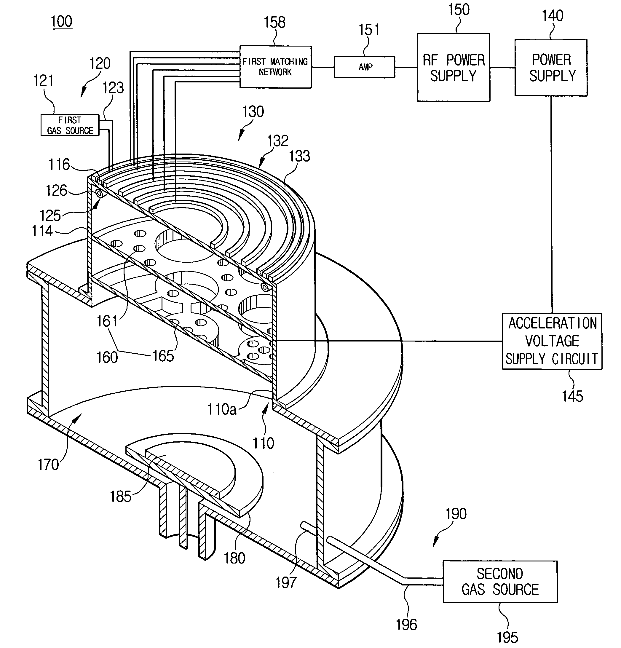
[0039]FIG. 5 is a schematic cut-away perspective view showing a plasma processing system 100 including a plasma accelerating apparatus according to an exemplary embodiment of the present invention.

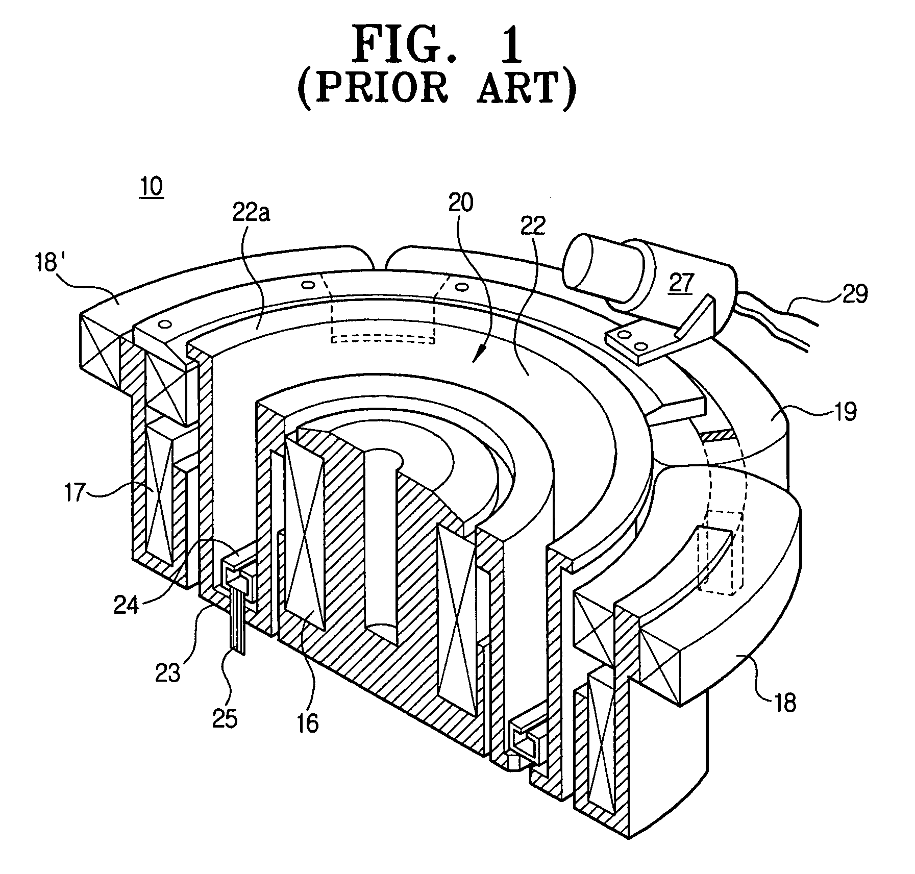
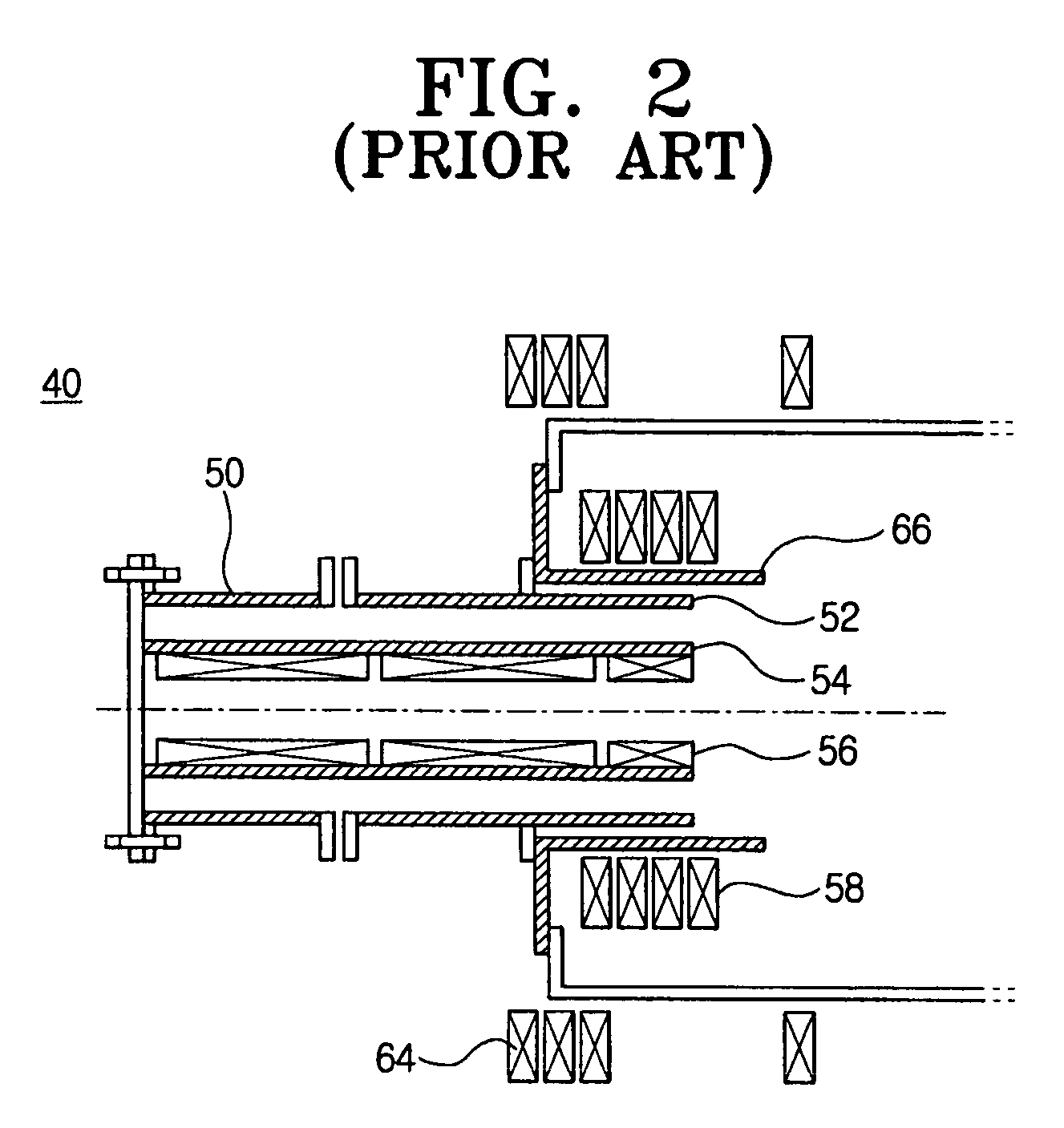
[0040] The plasma processing system 100 is a plasma etcher that forms a selective etching pattern on a substrate 185 by evaporating or ashing a thin film such as photoresist coated on the substrate using high temperature ionized plasma to remove the thin film from the substrate.

[0041] Referring to FIG. 5, the plasma processing system 100 includes a plasma channel 110, a first gas supply portion 120, a plasma generator 130, a plasma accelerating portion 160, a process chamber 170, and a second gas supply portion 190. The plasma channel 110, the first gas supply portion 120, the pl...


PUM


Abstract

A plasma accelerating apparatus and a plasma processing system, which efficiently elevate a drift velocity of a plasma beam and are simple to manufacture and simple in construction. A channel includes an outlet port opening at an end of the channel. A gas supply portion supplies a gas in the channel. A plasma generator provides ionization energy to the gas in the channel to generate a plasma beam. A plasma accelerating portion includes a plurality of grids transversely arranged spaced apart from each other by a predetermined distance in the channel for accelerating the plasma beam generated by the plasma generator to the outlet port of the channel with an electric field. The plasma accelerating apparatus and the plasma processing system elevate a drift velocity of the plasma beam more efficiently than conventional accelerating apparatuses that use an electromagnetic force induced by a magnetic field and a secondary current.

Description

CROSS-REFERENCE TO RELATED APPLICATIONS [0001] This application claims the benefit of priority under 35 U.S.C. § 119(a) from Korean Patent Application No. 10-2005-0069279, filed on Jul. 29, 2005 in the Korean Intellectual Property Office, the entire contents of which are incorporated herein by reference. BACKGROUND OF THE INVENTION [0002] 1. Field of the Invention [0003] Apparatuses consistent with the present invention relate to a plasma accelerating, and more particularly, to a plasma accelerating apparatus and a plasma processing system having the same, which are used for semiconductor substrate processing for etching and removing a thin film from a substrate or depositing the thin film on the substrate. [0004] 2. Description of the Related Art [0005] In recent years, with the increased need for high speed microprocessors and high recording density memories, techniques for reducing a thickness of a gate dielectric substance and a lateral size of a logic element has been actively ...

Claims


Application Information

Patent Timeline
Patent Type & Authority Applications(United States)
IPC IPC(8): H01J7/24
CPCH01J27/024H01J27/143H05H1/54H01J37/32357H01J37/321
Inventor LEE, WON-TAE
Owner SAMSUNG ELECTRONICS CO LTD
Why Eureka
Try Eureka