Gated nanorod field emitter structures and associated methods of fabrication

a nanorod and emitter technology, applied in the manufacture of electrode systems, electric discharge tubes/lamps, tubes with electrostatic control, etc., can solve the problems of limiting the operation life of fluorescent lighting, low pressure gas discharge lighting and fluorescent lighting, and reducing power consumption/dissipation

Active Publication Date: 2007-02-08
GENERAL ELECTRIC CO
View PDF12 Cites 27 Cited by
  • Summary
  • Abstract
  • Description
  • Claims
  • Application Information

AI Technical Summary

Benefits of technology

[0008] Embodiments of the present invention provide novel methods for fabricating novel cold cathode field emitter devices, wherein such devices comprise an array of emitter tips that are self-aligned with their respective gates and decouples the emitter-to-tip spacing from the dielectric support for the gate layer, thereby providing a relatively high emitter tip density. Such methods are relatively simple, cost-effective, and efficient; and, they provide field emission devices that are suitable for use in x-ray imaging applications, lighting applications, flat panel field emission display (FED) applications, etc. Invention embodiments are also directed to the gated nanorod field emission devices made by the above-mentioned methods.

Problems solved by technology

Moreover, applications like low pressure gas discharge lighting and fluorescent lighting, which are limited by the life of the thermionic emitters that are typically used, will benefit from cold cathode field emitters.
Typically, the smaller the emitter tip-to-gate distance, the lower the turn-on voltage of the cold cathode field emitter and the lower the power consumption / dissipation.
The resulting ions bombard the emitter tips and damage their sharp points, decreasing the emission current of the cold cathode field emitter over time and limiting its operating life.
This, however, has the negative consequence of increasing the capacitance between the cathode electrode and the gate electrode, thus increasing the response time of the cold cathode field emitter.
Generally, optical lithography and other methods are limited to field openings on the order of about 0.5 microns or larger and emitter tip-to-gate distances on the order of about 1 micron or larger.

Method used


Image

  • Gated nanorod field emitter structures and associated methods of fabrication
  • Gated nanorod field emitter structures and associated methods of fabrication
  • Gated nanorod field emitter structures and associated methods of fabrication

Examples


example 1

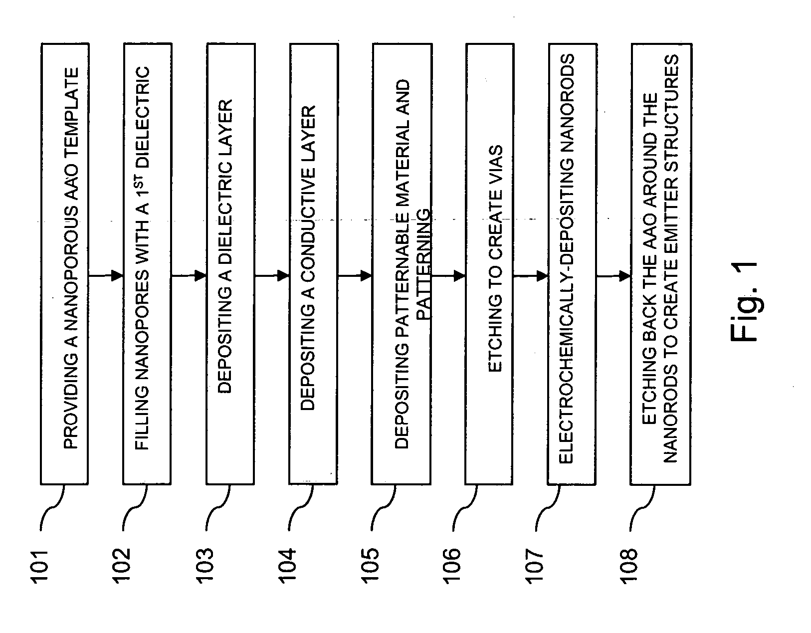
[0116] This Example serves to illustrate fabrication of a gated field emitter device (e.g., device 133, shown in FIG. 13), in accordance with some embodiments of the present invention.

[0117] A Si wafer was cleaned using a KEROS (peroxide and sulfuric acid clean also known as a piranha etch) and HF dip. On the cleaned wafer various layers were deposited in the following order and with the following thicknesses: 200 Å TiW / 500 Å Au / 60 Å Ti / 1 μm Al. The TiW was used as an adhesion layer, Au as the conductive layer, and Ti as the sacrificial barrier layer. The Al in this layered stack was then anodized to create nanoporous AAO. During this process, the top Ti layer oxidized to form insulating TiOx (sacrificial barrier layer). The TiOx sacrificial barrier layer was etched using a wet etching solution (80 parts H2O: 1 part HF: 1 part H2O2) for 30 seconds. Upon removal of the TiOx, the nanopores in the nanoporous AAO extend down to the conductive Au layer and form a template in which nanor...

example 2

[0123] This Example serves to illustrate fabrication of a gated field emitter device (e.g., devices 3500 and 3900, shown in FIGS. 35 and 39, respectively), in accordance with some embodiments of the present invention.

[0124] A Si wafer was cleaned using a KEROS and HF Dip. On the cleaned wafer various layers were deposited in the following order and with the following thicknesses: 200 Å TiW / 500 Å Cu / 150 Å Ti / 1 μm Al. The TiW was used as an adhesion layer, Au as the conductive layer, and Ti as the sacrificial barrier layer. The Al in this layered stack was then anodized to create a substrate supported nanoporous AAO template. During this process, the top Ti layer of the stack is oxidized to form insulating TiOx (sacrificial barrier layer).

[0125] Spin-on-glass (SOG) was applied to the top of the nanoporous AAO template and then annealed at 425° C. for 30 minutes with a 2 hour cool. The SOG was then etched from the surface using ICP for 5.5 minutes (time is dependent on SOG thickness)...

example 3

[0126] This Example serves to illustrate fabrication of a gated field emitter device (e.g., devices 3500 and 3900, shown in FIGS. 35 and 39, respectively), in accordance with some embodiments of the present invention.

[0127] A Si wafer was cleaned using a KEROS and HF Dip. On the cleaned wafer various layers were deposited in the following order and with the following thicknesses: 200 Å TiW / 500 Å Cu / 150 Å Ti / 1 μm Al. The TiW was used as an adhesion layer, Cu as the conductive layer, and Ti as the sacrificial barrier layer. The Al in this layered stack was then anodized to create a substrate supported nanoporous AAO template. During this process, the top Ti layer of the stack is oxidized to form insulating TiOx (sacrificial barrier layer). Note that this sacrificial barrier layer is formed in all of the Examples presented herein.

[0128] Spin-on-glass (SOG) was applied to the top of the nanoporous AAO template and then annealed at 425° C. for 30 minutes with a 2 hour cool. The SOG was...


PUM


Abstract

The present invention relates to gated nanorod field emission devices, wherein such devices have relatively small emitter tip-to-gate distances, thereby providing a relatively high emitter tip density and low turn on voltage. Such methods employ a combination of traditional device processing techniques (lithography, etching, etc.) with electrochemical deposition of nanorods. These methods are relatively simple, cost-effective, and efficient; and they provide field emission devices that are suitable for use in x-ray imaging applications, lighting applications, flat panel field emission display (FED) applications, etc.

Description

[0001] This invention was made with support from the United States Department of Commerce, National Institute of Standards and Technology (NIST) Contract No. 70NANB2H3030.TECHNICAL FIELD [0002] The present invention relates generally to field emission devices that are suitable for use in x-ray imaging applications, lighting applications, flat panel field emission display applications, microwave amplifier applications, electron-beam lithography applications and the like. More specifically, the present invention relates to gated nanorod field emission devices and associated methods of fabrication. BACKGROUND INFORMATION [0003] Electron emission devices, such as thermionic emitters, cold cathode field emitters and the like, are currently used as electron sources in x-ray tube applications, flat panel field emission display applications, microwave amplifier applications, electron-beam lithography applications and the like. Typically, thermionic emitters, which operate at relatively high...

Claims


Application Information

Patent Timeline
Patent Type & Authority Applications(United States)
IPC IPC(8): H01J1/02B05D5/12H01J9/04
CPCH01J1/304H01J9/025H01J3/021H01J1/3044
Inventor HUDSPETH, HEATHER DIANELEE, JI UNGCORDERMAN, REED ROEDERZHANG, ANPINGROHLING, RENEE BUSHEYDENAULT, LAURAINEBALCH, JOLEYN EILEEN
Owner GENERAL ELECTRIC CO
Why Eureka
Try Eureka