Notably,
mask 18 may not be “perfect,” due to its own manufacturing process.
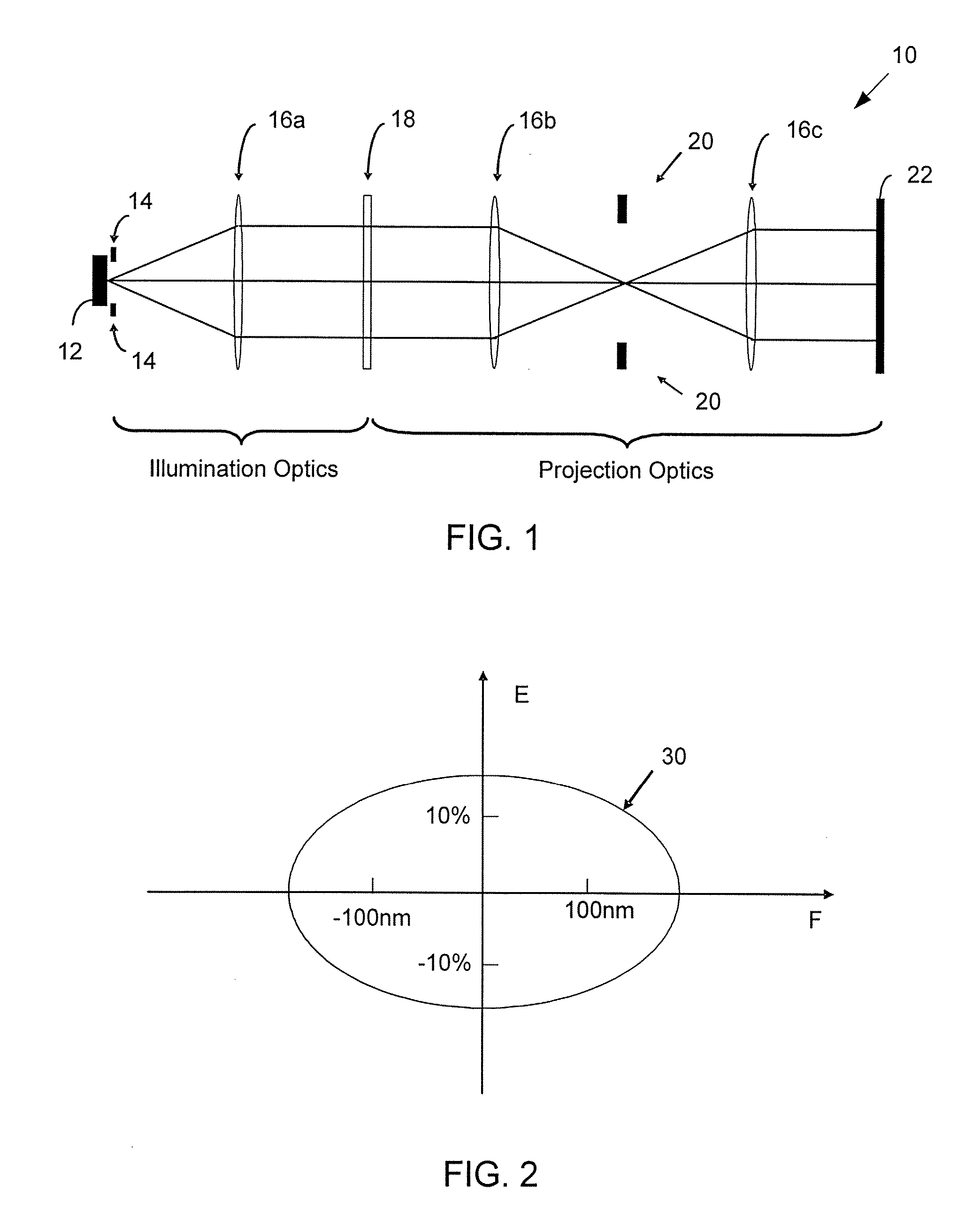
Due to the
wavelength of light being finite, and current techniques employing wavelengths that are larger than the minimum linewidth that is printed on wafer 22, there are typically significant light interference and
diffraction effects affecting the imaging process.
When the resist is exposed by the projected image and thereafter baked and developed, the resist tends to undergo complex chemical and physical changes.
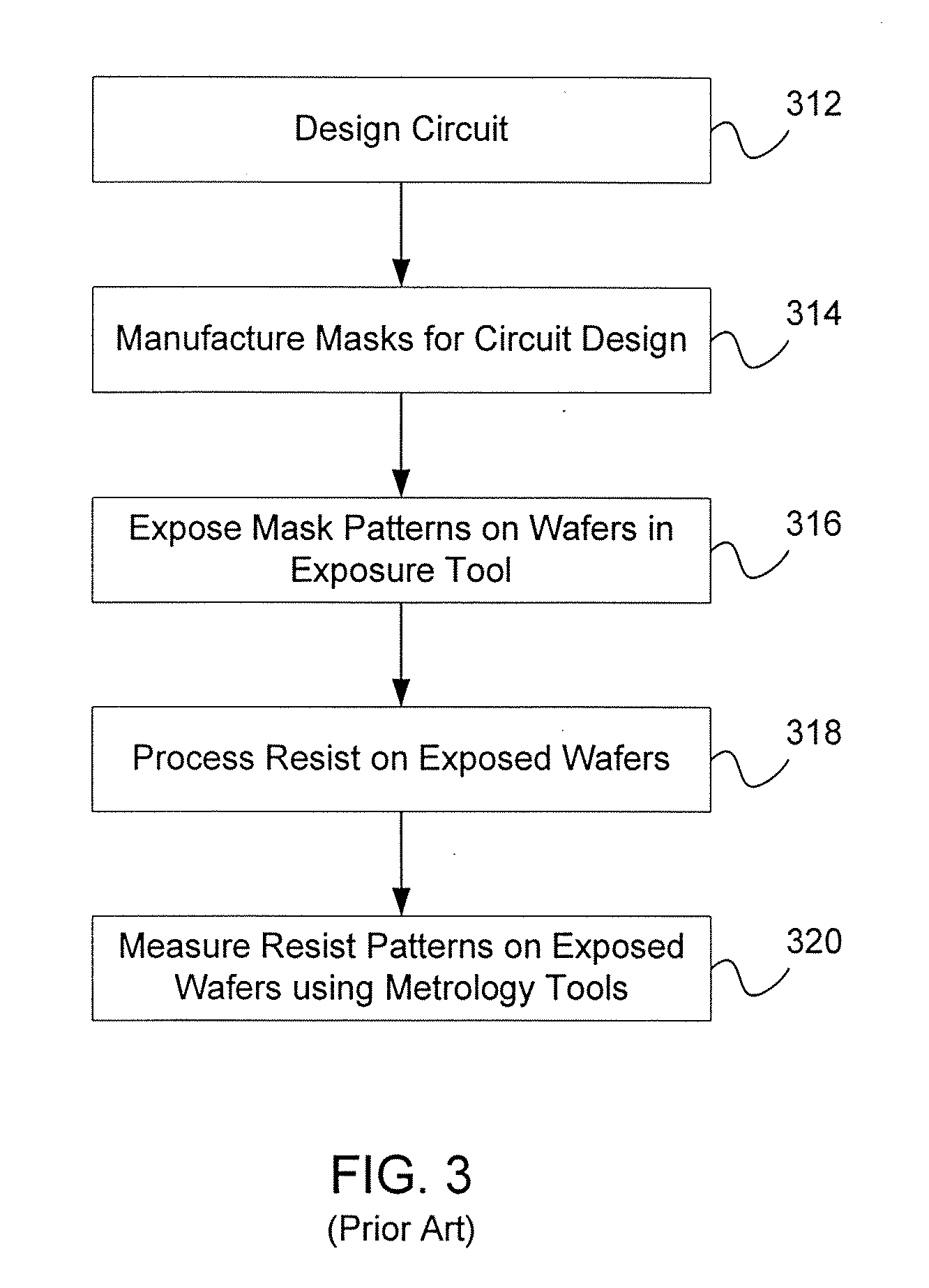
The time and expense needed to create test masks,
expose them, process test wafers and determine the final dimensions experimentally would be prohibitive without the savings in time and
processing cost made possible by
simulation.
In developing and calibrating the models used for all aspects of lithography simulation, one of the most difficult challenges has been the correct separation of the model into its optical and resist components, where the optical model module accurately represents the formation of the aerial image by the
exposure tool and the resist model module accurately represents the absorption of the incident aerial image by the resist as well as the development of the exposed resist to form the final three-dimensional resist pattern.
Assuming that the measured data are sufficiently accurate, any differences between the model predictions for the resist patterns and the measurements of the actual resist patterns could be due to inaccuracy in either the resist model or the optical model.
Selection of a non-optimal parameter set often results in incomplete convergence of the
model fitting procedure, or, if the
model fitting does converge, the values to which the parameters converge often have little relationship to
physical reality and therefore provide limited
predictability.
In this current environment, the
model prediction may be optimized for a restricted set of
calibration test patterns, but the terms in the model may not be correct, leading to incorrect predictions of patterns that were not included in the set of
calibration test patterns.
In addition, if a model is calibrated without achieving a significant match between
model parameters and real physical parameters, model
predictability will be limited in the following respect: if one specific parameter is deliberately changed in the process, such as the
partial coherence (sigma) of the illuminator or the
numerical aperture (NA) of the
projection lens, simply changing that parameter in the model will most likely not give the correct results.
In many cases, developers of lithography simulation models have recognized the difficulty in developing truly separable models and have tacitly admitted that the
model parameters do not bear a unique one-to-one correspondence with the physical parameters for which they are named.
As a result, if any term in the real physical process is deliberately changed, it is not sufficient to change the one corresponding term in the model.
This indicates that such models and the methods used to calibrate the models do not achieve true, physically significant model separation.
As a result, any change in the process requires extensive,
time consuming model recalibration.
The use of non-separable models means that an OPC model that is optimized for a given exposure tool and a given resist process is not easily transferable to another tool or another resist process.
Efforts to implement workable first-principle models have been largely unsuccessful due to a number of factors: the large number of resist parameters required to accurately describe the complex
kinetics of acid and base
diffusion in modern
acid catalyzed resist systems as well as the surface and substrate interaction effects in these resists; the sensitivity to the various bake temperatures and thermal cycles; the difficulty in accurately modeling the development path at the developer-resist interface, where the resist film undergoes a complex phase transformation from
solid to soluble gel; and the
molecular level perturbations of the acid and base species in the resist which gives rise to stochastic
line edge roughness (see “
Resist Blur and
Line Edge Roughness,” G. Gallatin, Optical Microlithography XVIII, B. W. Smith, editor, Proc.
Even if a microscopic resist model could be simplified from the
physical reality to a manageable set of parameters, the linkage between the resist model and optical model is still difficult to break due to the lack of understanding of the exact optical conditions in the exposure tool.
These deviations from idealized theory can cause extensive proximity effects which are difficult to separate from resist
processing effects.

