Method of packaging and interconnection of integrated circuits

a technology of integrated circuits and interconnections, applied in the field of electronic packaging, can solve the problems of less than optimal performance of such devices, less well-developed and expensive process for fabricating such devices, and many problems in the handling of such thin (and therefore delicate) chips, and achieve the effect of high density and enhanced adhesion between the two substrates

Inactive Publication Date: 2007-02-22
INTELLEFLEX CORP +1
View PDF19 Cites 15 Cited by
  • Summary
  • Abstract
  • Description
  • Claims
  • Application Information

AI Technical Summary

Benefits of technology

[0011] The present invention provides a low temperature, high density IC flip chip packaging concept in which the surface of the IC chip is in intimate contact with the surface of the substrate. The IC packaging process of the present invention is based on the use of amalgams, which are mixtures of metallic elements that are liquid when first mixed, but which harden into high-melting metallic solids upon curing. In the present invention, one substrate is provided with raised contact pads, and the other substrate is pr

Problems solved by technology

However, the performance of such devices tends to be less than optimal, and the processes for fabricating them less well developed and more costly than for the well-known processes of fabricating transistors in silicon wafers.
In practice, many problems arise in the handling of such thin (and therefore delicate) chips.
However, apart from the possibility of defects arising from incomplete filling of the holes, this process does not result in a highly planar surface due to variations in the thickness of chips coupled with variations in the depth of the depressions, and there is still a small but significant gap between the side of the chip and the side of the hole.
This leads to complexity in forming the subsequent interconnect metallization.
It also does not address the issue of reliability du

Method used


Image

  • Method of packaging and interconnection of integrated circuits
  • Method of packaging and interconnection of integrated circuits
  • Method of packaging and interconnection of integrated circuits

Examples


Embodiment Construction

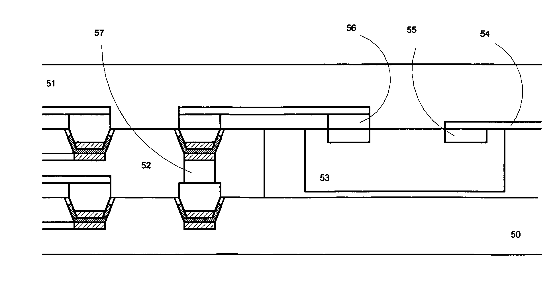
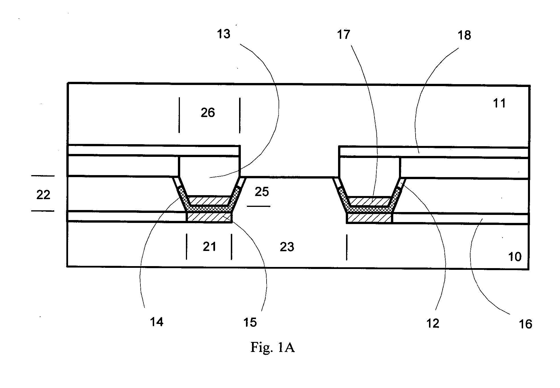
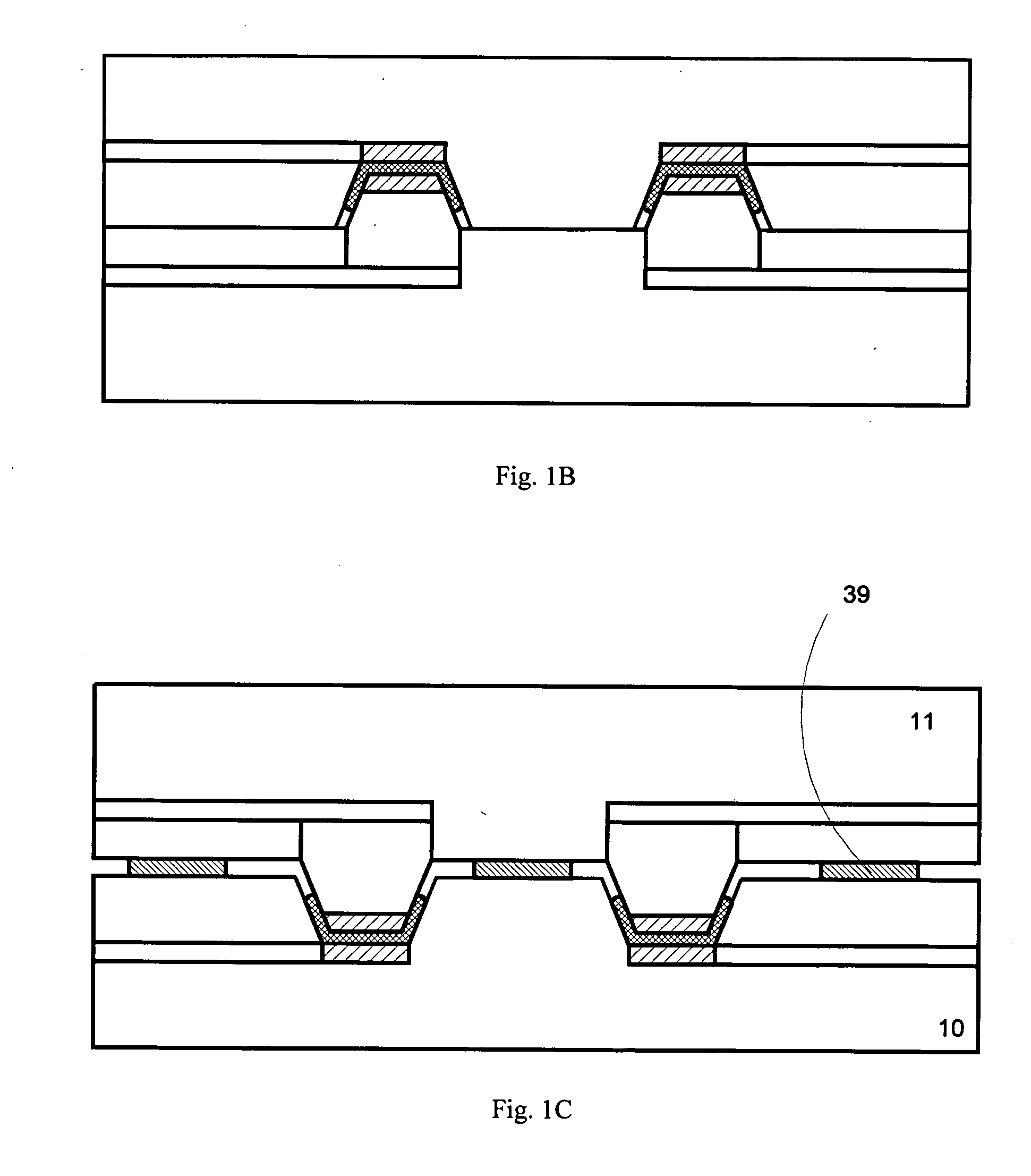
[0021] The present invention provides a novel IC packaging concept for flip chip packaging and substrate lamination. The present invention provides the ability to bond chips face down onto connection pads, in a manner similar to conventional flip-chip bonding (see FIGS. 1A-1C). Alternatively, the present invention packaging process can laminate two circuitry-bearing substrates together, one of which bears chips, with a third film in between, and have electrical connections between the two substrates (see FIGS. 1D-1E). The contact density can be micron-scale density, since the separation between the two substrates (or between the surfaces of the chips and the mating substrate) can be as small as desired, perhaps as small as one micron or less, and the contact pads can have a lateral size of the order of one micron and spacing between pads of the order of one micron. These capabilities provide significant advantages over conventional flip chip technology.

[0022] Further, the present i...


PUM


Abstract

A semiconductor chip packaging on a flexible substrate is disclosed. The chip and the flexible substrate are provided with corresponding raised and indented micron-scale contact pads with the indented contact pads partially filled with a liquid amalgam. After low temperature amalgam curing, the chip and the substrate form a flexible substrate IC packaging with high conductivity, controllable interface layer thickness, micron-scale contact density and low process temperature. Adhesion between the chip and the substrate can be further enhanced by coating other areas with non-conducting adhesive.

Description

FIELD OF THE INVENTION [0001] The present invention is related generally to electronics packaging and, more particularly to packaging and interconnection of integrated circuits on a flexible substrate. BACKGROUND OF THE INVENTION [0002] Board level semiconductor packaging and interconnection of integrated circuits (IC) is the process to electrically connect the IC chips to each other and to external circuitry to function as an electronic system. The IC chips have input and output contact pads and the interconnection is typically an array of metallic connections within a support substrate. The normal packaging process of forming a fully functional product based on integrated circuits usually includes placing the semiconductor IC chips on a printed circuit board (PCB) and soldering their contact pads to contact pads on the PCB. Several connection techniques are widely used and well known in the art. These include wire bonding, tape automated bonding (TAB), flip-chip bonding, etc. [000...

Claims


Application Information

Patent Timeline
IPC IPC(8): H01L23/48
CPCH01L21/4867H01L23/4985H01L23/49866H01L24/11H01L24/13H01L24/16H01L24/81H01L24/90H01L25/0655H01L2224/1132H01L2224/114H01L2224/116H01L2224/13099H01L2224/81136H01L2224/81801H01L2224/90H01L2924/01012H01L2924/01013H01L2924/01022H01L2924/01025H01L2924/01027H01L2924/01029H01L2924/0103H01L2924/01032H01L2924/01042H01L2924/01047H01L2924/01049H01L2924/01051H01L2924/01074H01L2924/01078H01L2924/01079H01L2924/14H01L2924/1532H01L2924/19041H01L2924/19042H01L2924/19043H05K3/3452H05K3/3463H01L2224/16237H01L2224/81141H01L2224/05571H01L2224/05794H01L2224/05839H01L2224/05844H01L2224/05847H01L2224/81097H01L2924/01006H01L2924/01023H01L2924/01024H01L2924/01033H01L2924/0105H01L2924/014H01L2224/81099H01L2224/05705H01L2224/05824H01L2224/0582H01L2224/05857H01L2224/05871H01L2224/0588H01L2224/05869H01L2224/0586H01L2224/05855H01L2224/05849H01L2224/05884H01L2224/05866H01L2224/05872H01L2224/05811H01L2224/058H01L2924/0108H01L2924/00014H01L2924/0001H01L2924/10253H01L2924/00H01L2224/0401H01L2924/0002H01L2224/05552H01L24/05
Inventor SHEATS, JAMES
Owner INTELLEFLEX CORP
Why Eureka
Try Eureka