Mobility enhancement in SiGe heterojunction bipolar transistors

a bipolar transistor and heterojunction technology, applied in the field of mobility enhancement of sige-based heterojunction bipolar transistors, can solve the problems increasing the carrier scattering, carrier trapping, and carrier recombination, and no longer contain elastic energy stored in the distorted sige crystal structure. , to achieve the effect of increasing the biaxial strain in the base region, improving the performance of currently available sige-based hbt devices,

Inactive Publication Date: 2007-03-01
GLOBALFOUNDRIES INC
View PDF87 Cites 2 Cited by
  • Summary
  • Abstract
  • Description
  • Claims
  • Application Information

AI Technical Summary

Benefits of technology

[0008] The present invention seeks to further improve performance of currently available SiGe-based HBT devices by increasing biaxial strain in the base region of the HBT devices, which in turn increases carrier mobility in the base region.
[0009] The present invention discovers that although a further increase in the Ge content of the ultra-thin base layers of the currently available SiGe-based HBT devices does not further increase carrier velocity, it can cause increase in biaxial strains near the base region, i.e., increased compressive strain along the direction parallel to the substrate surface (i.e., the lateral direction) and increased tensile strain along the direction perpendicular to the substrate surface (i.e., the vertical direction), which functions to enhance mobility of holes laterally flowing through the base region and electrons vertically traversing the base region.
[0010] Since the carrier base-transit time depends not only on carrier velocity, but also on carrier mobility, the carrier base-transit time of the currently available SiGe-based HBT devices can be further reduced by increasing the Ge content of the ultra-thin base layers of such HBT devices to near-critical value.
[0011] Further, the base resistance of the SiGe-based HBT devices also depends on the carrier mobility, so an increase of the base layer Ge content to near-critical value can also be used to reduce the base resistance.
[0014] Critical germanium content for the ultra-thin SiGe-containing layer can be readily calculated by various conventionally known methods, as described hereinafter in greater detail, and the present invention selects the average calculated critical germanium content for controlling the actual germanium content in the SiGe-containing layer, so as to minimize the risk of dislocation generation. For example, for a SiGe-containing layer of about 50 nm thick, the calculated critical germanium content is between about 16 atomic % to about 18 atomic %, while the average value of 17 atomic % is selected as the predetermined critical germanium content in the present invention. For another example, the calculated critical germanium content of a 100 nm thick SiGe-containing layer is between about 9 atomic % to about 11 atomic %, and the average value of 10 atomic % is selected as the predetermined critical germanium content for practice of the present invention.
[0019] Therefore, a uniform increase in the Ge content across the ultra-thin SiGe-containing base layer can be used to reach near-critical Ge content in the base layer, thereby maximizing the biaxial strain and the carrier mobility in the base layer, but it does not change the Ge grading rate or the shape of the Ge content profile and thus maintains the same quasi-static drift field in the base layer.

Problems solved by technology

However, when the strain in the pseudomorphically grown SiGe film reaches a critical level, either due to increase of the SiGe film thickness or increase of the Ge content, it can no longer be contained by elastic energy stored in the distorted SiGe crystal structure.
Dislocation defects originated from strain relaxation are electrically active and can cause increased carrier scattering, carrier trapping, and carrier recombination.
In other words, increased Ge grading in the ultra-thin base layers does not yield further improvements in carrier velocity.

Method used


Image

  • Mobility enhancement in SiGe heterojunction bipolar transistors
  • Mobility enhancement in SiGe heterojunction bipolar transistors
  • Mobility enhancement in SiGe heterojunction bipolar transistors

Examples


Embodiment Construction

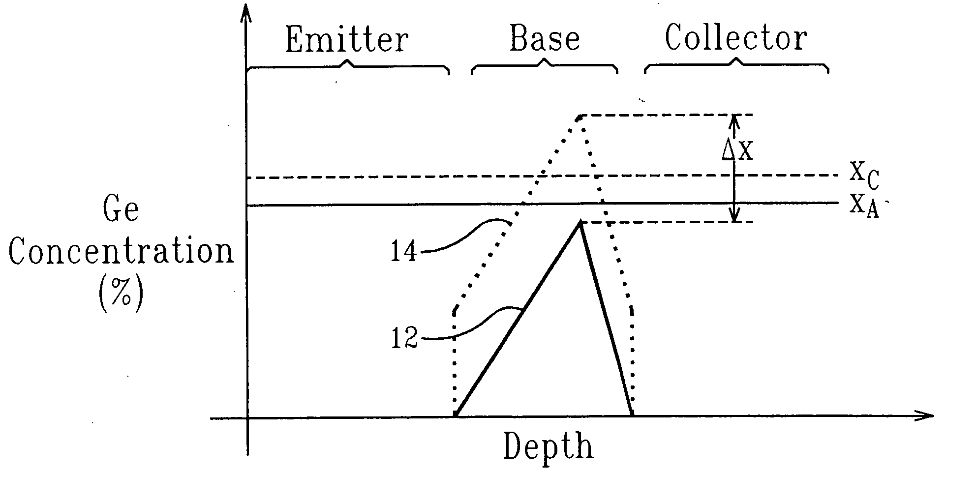
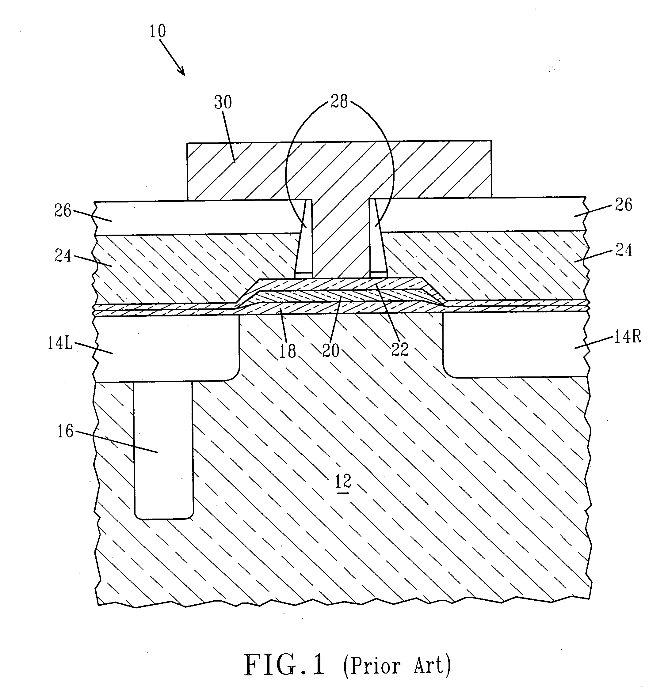
[0039] A typical SiGe-based HBT having a deep trench isolation and a T-shaped emitter is shown in FIG. 1 (hereinafter FIG. 1). Specifically, FIG. 1 includes a semiconductor structure 10 that includes at least a collector 12 that is positioned between two shallow trench isolations regions 14R and 14L. The shallow trench isolation region on the left hand side of the drawing, represented by 14L, has a deep trench 16 extending from a bottom walled surface of the shallow trench. The semiconductor structure shown in FIG. 1 also includes a first epitaxial silicon layer 18, a SiGe base 20, and a second epitaxial silicon layer 22, which are located atop the trench isolation regions and the collector 12. The structure shown in FIG. 1 also includes an extrinsic base 24 and an oxide layer 26 which are patterned to expose a surface of the second epitaxial silicon layer 22 that is located above the SiGe base 20. Nitride spacers 28 are located on sidewalls of the oxide layer 26 and the extrinsic b...


PUM


Abstract

The present invention relates to a high performance heterojunction bipolar transistor (HBT) having a base region with a SiGe-containing layer therein. The SiGe-containing layer is not more than about 100 nm thick and has a predetermined critical germanium content. The SiGe-containing layer further has an average germanium content of not less than about 80% of the predetermined critical germanium content. The present invention also relates to a method for enhancing carrier mobility in a HBT having a SiGe-containing base layer, by uniformly increasing germanium content in the base layer so that the average germanium content therein is not less than 80% of a critical germanium content, which is calculated based on the thickness of the base layer, provided that the base layer is not more than 100 nm thick.

Description

FIELD OF THE INVENTION [0001] The present invention relates to a SiGe-based heterojunction bipolar transistor, and more particularly, to a SiGe-based heterojunction bipolar transistor that has improved performance due to mobility enhancement. The present invention is also related to a method of fabricating such a SiGe-based heterojunction bipolar transistor. BACKGROUND OF THE INVENTION [0002] In the state-of-the-art SiGe heterojunction bipolar transistor (HBT) devices, the base material is epitaxially deposited by means of chemical vapor deposition (CVD) or molecular beam epitaxy (MBE) as front-end-of-line (FEOL) films relatively early in the manufacturing process. This offers the possibility of tailoring specific base profiles in both alloy and dopant and allows pseudomorphic growth of alloys of silicon with germanium and carbon, which can be used to improve performance of the HBT devices. [0003] Specifically, incorporation of substitutional germanium into the crystal lattice of th...

Claims


Application Information

Patent Timeline
Patent Type & Authority Applications(United States)
IPC IPC(8): H01L29/00
CPCH01L29/161H01L29/7378H01L29/165H01L29/00
Inventor ADAM, THOMASCHIDAMBARRAO, DURESETI
Owner GLOBALFOUNDRIES INC
Why Eureka
Try Eureka