

Transparent material processing with an ultrashort pulse laser
a technology transparent material, which is applied in the field of ultrashort pulse laser processing, can solve the problems of poor cleave process precision, low quality of cleave facets, and additional interaction, and achieve the effects of reducing the degree of localization of weld features, reducing the thickness of the material through which the beam can be focused, and increasing linear absorption
- Summary
- Abstract
- Description
- Claims
- Application Information
AI Technical Summary
Benefits of technology
Problems solved by technology
Method used
Image

Examples
Embodiment Construction
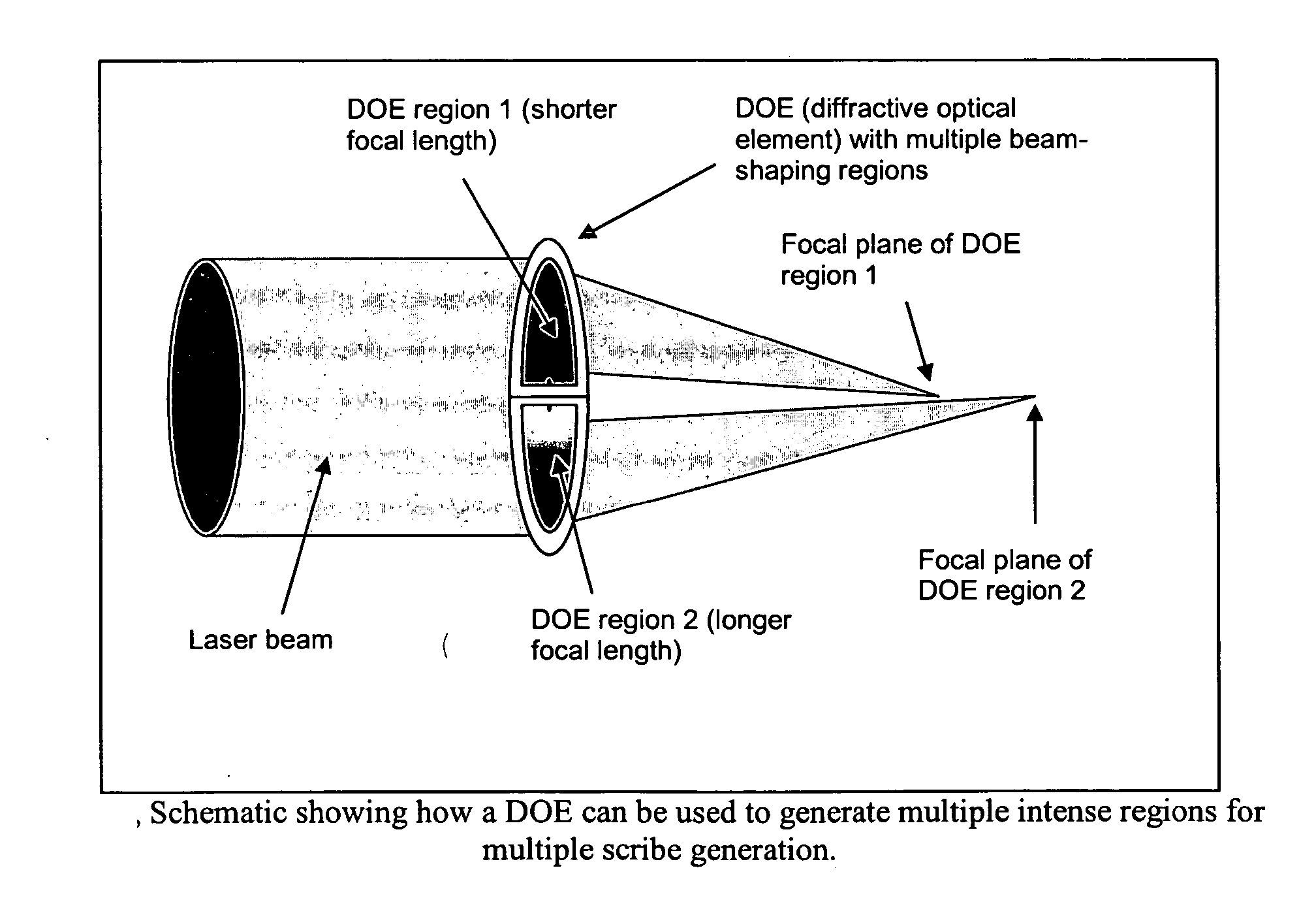
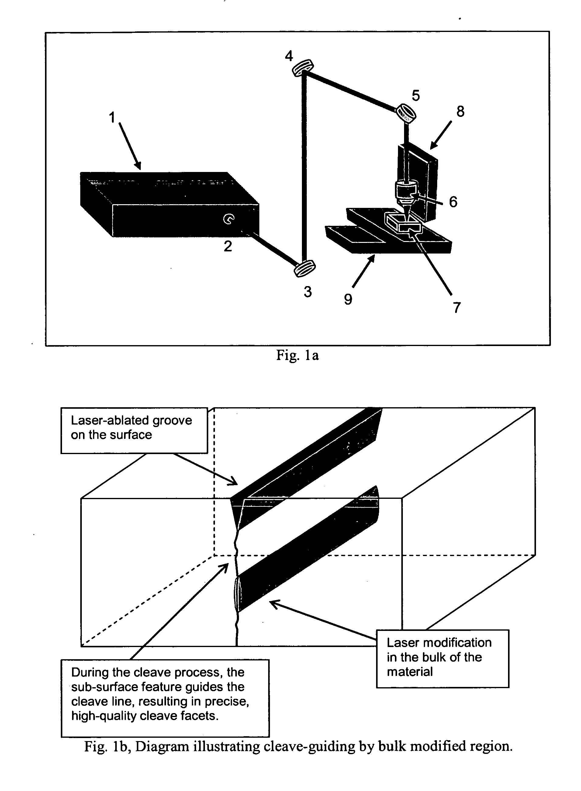
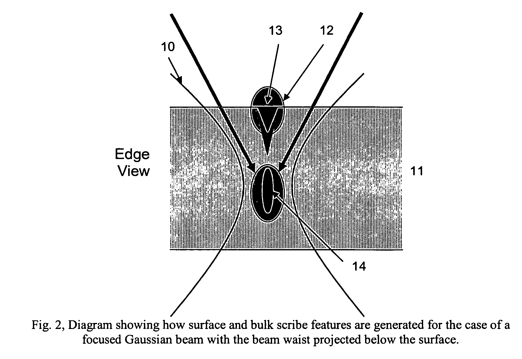
[0067] 1. Ultrashort Pulse Laser Scribing
[0068]FIG. 1 illustrates one embodiment of the current invention, which is a method for scribing transparent materials for subsequent cleaving. This embodiment employs a laser system (1) producing a beam of ultrashort laser pulses (2), an optical system (6) that generates a desired laser beam intensity distribution, and a target material (7) to be scribed that is transparent to the wavelength of the laser pulses. In addition, a Z-axis stage (8) is used for beam focus position control (depth), and an automated X-Y axis stage assembly (9) is generally required for moving the work pieces (7) laterally relative to the focused laser beam. Alternatively, the laser beam (2) could be moved relative to a stationary target material with the use of scanning mirrors (3), (4), and (5).
[0069] The laser beam (2) is directed through the optical system (6), which transforms the laser beam (2) to create a desired 3-dimensional intensity distribution. Particu...
PUM
| Property | Measurement | Unit |
|---|---|---|
| melting temperature | aaaaa | aaaaa |
| melting temperature | aaaaa | aaaaa |
| distance | aaaaa | aaaaa |
Abstract
Description
Claims
Application Information