Three-terminal switch array, three-terminal switch array device, combined semiconductor device, and image form appartus

a switch array and three-terminal technology, applied in the field of three-terminal switch arrays, can solve the problems of increasing the the cost of wire bonding, and the difficulty of reducing the size and cost of the led head as much as would be desirable, so as to reduce the size of the combined semiconductor device

Inactive Publication Date: 2007-03-15
OKI DATA CORP
View PDF6 Cites 27 Cited by
  • Summary
  • Abstract
  • Description
  • Claims
  • Application Information

AI Technical Summary

Benefits of technology

[0057] An object of the present invention is accordingly to reduce the size of a combined se

Problems solved by technology

For reasons that will now be explained, it has proven difficult to reduce the size and cost of the LED head as much as would be desirable.
In the conventional scheme illustrated in FIG. 2, with separate LED array chips and driver chips, the cost of wire bonding and the size of the LED array chips and driver chips are major factors that drive up the cost of the LED head.
In particular, the material cost of the compound semiconductor LED array chips is high.
One factor in the comparatively large size of the LED array chips and driver chips is the large number of space-consuming bonding pads needed to interconnect them.
The conventional LED head disclosed in JP/2004-207444 permits the use of various compound semiconductor materials, such as GaAs, GaP, AlGaAs, InGaAsP, and InGaAlAs, for the light-emitting elements, but whichev

Method used


Image

  • Three-terminal switch array, three-terminal switch array device, combined semiconductor device, and image form appartus
  • Three-terminal switch array, three-terminal switch array device, combined semiconductor device, and image form appartus
  • Three-terminal switch array, three-terminal switch array device, combined semiconductor device, and image form appartus

Examples


first embodiment

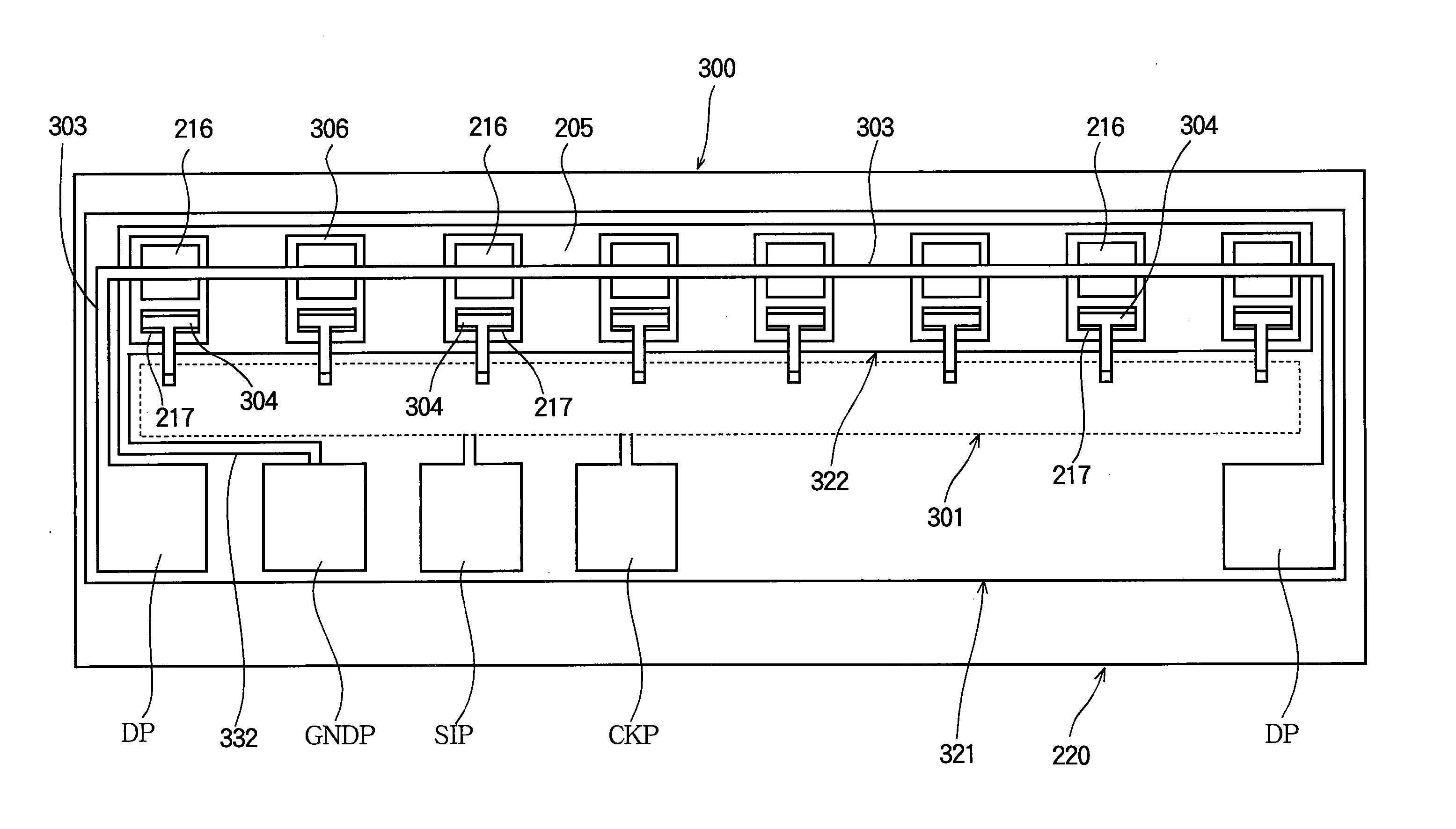
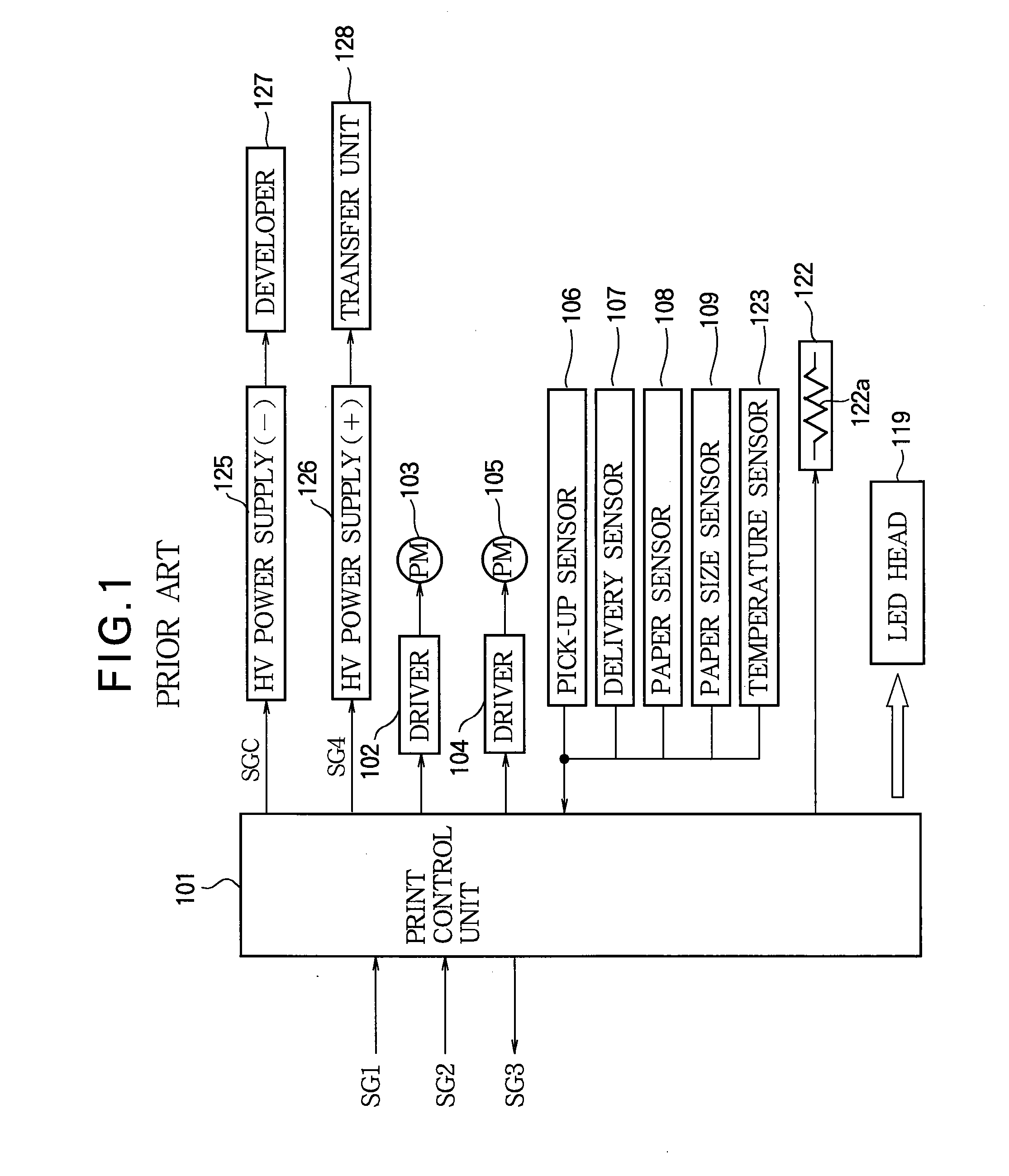
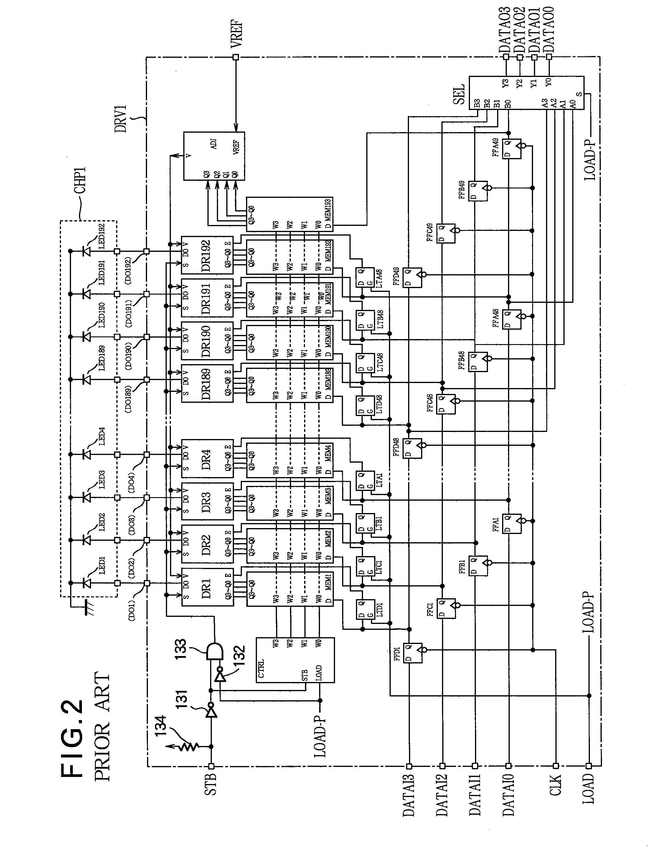
[0095] Referring to FIG. 10, the first embodiment of the invention is a three-terminal switch array device including a row of three-terminal switching elements d1-d8. The number of three-terminal switching elements is not limited to the eight shown. The three-terminal switching elements may be light-emitting thyristors, in which case the array will be referred to as a light-emitting thyristor array. A light-emitting thyristor array with one hundred ninety-two light-emitting thyristors instead of eight can be used to replace, for example, the LED array CHP1 in FIG. 2.

[0096] The three-terminal switching elements d1-d8 are formed from a thin film and are attached to a substrate 321 in a rectangular area 322. All of the three-terminal switching elements may be formed in a single thin film, or the three-terminal switching elements d1-d8 may be formed in separate thin films and attached individually to the substrate 321. Alternatively, the three-terminal switching elements may be dispose...

second embodiment

[0142] The second embodiment adds a gray-scale function to the configuration in the first embodiment.

[0143] Referring to the schematic circuit diagram in FIG. 18, the second embodiment includes the combined semiconductor device 300 described in the first embodiment (FIG. 10), and a driving circuit 326. For electrophotographic printing applications, normally there will be an array of combined semiconductor devices 300 mounted on a printed circuit board as in FIG. 16. The driving circuit 326 may form part of the print control unit 101 shown in FIG. 1, for example, or equivalent print control block in an electrophotographic printer.

[0144] The driving circuit 326 includes a digital-to-analog (D / A) converter 401 that converts an eight-bit parallel digital input signal (D7-D0) to an analog current value for output from a driving current output terminal IOUT. The output current (D) accordingly has 256 selectable levels. The D / A converter 401 can be any device of the current output type, ...

third embodiment

[0161] In the third embodiment, the light-emitting thyristors are disposed on a side surface of the combined semiconductor device.

[0162] Referring to FIG. 20A, the light-emitting thyristor unit 540 in the third embodiment includes a plurality of combined semiconductor devices 500 mounted on a printed circuit board 220 to which they are electrically coupled via bonding wires 221 and pads 229 as in the preceding embodiments, but no thyristor epi-films are disposed on the upper surfaces of the combined semiconductor devices 500. Instead, the thyristor epi-films 306 are located as shown in FIG. 20B, on side surfaces or edges of the combined semiconductor devices 500. These side surfaces will also be referred to as the first surfaces of the combined semiconductor devices.

[0163] As in the preceding embodiments, each combined semiconductor device 500 has a silicon substrate in which a shift register (not shown) is formed, and electrodes or bonding pads 505 on which the bonding wires 221 ...


PUM


Abstract

An array of three-terminal switching elements such as light-emitting thyristors is formed from a thin semiconductor film. A combined semiconductor device may be formed by bonding the thin-film three-terminal switching elements to a major surface or edge surface of an integrated circuit chip including a shift register that shifts data supplied to the control electrodes of the three-terminal switching elements, or by bonding both the thin-film three-terminal switching elements and another thin semiconductor film including the shift register to a substrate. In either case, thin-film wiring may be used to interconnect the shift register and the switching elements, and the need for an array of large transistors to feed driving current to the switching elements is eliminated, reducing the size and cost of the combined semiconductor device, which can be advantageously used in the optical head of an electrophotographic printer.

Description

BACKGROUND OF THE INVENTION [0001] 1. Field of the Invention [0002] The present invention relates to an array of three-terminal switches formed in a thin semiconductor film, such as an array of light-emitting thyristors formed in a thin compound semiconductor film; to a combined semiconductor device combining this type of thin-film array and its driving circuitry; and to an image-forming device having combined semiconductor devices of the invented type. [0003] 2. Description of the Related Art [0004] Arrays of light-emitting elements are used as light sources in electrophotographic printers. In a conventional electrophotographic printer of this type, the light-emitting elements are light-emitting diodes (LEDs) that form an electrostatic latent image by selectively illuminating a charged photosensitive drum responsive to print data. The image is then developed by applying toner to the photosensitive drum, the toner image is transferred from the photosensitive drum onto paper, and the...

Claims


Application Information

Patent Timeline
IPC IPC(8): H01L29/10H01L33/30H01L33/58H01L33/08H01L33/62
CPCB41J2/45H01L25/167H01L2224/48227H01L2924/01046H01L2924/01079H01L2924/09701H01L2924/01019H01L2924/1301H01L2924/10253H01L2924/00H01L2924/12044
Inventor NAGUMO, AKIRA
Owner OKI DATA CORP
Why Eureka
Try Eureka