Apparatus for preparation of silicon crystals with reduced metal content

a silicon crystal and metal content technology, applied in the direction of crystal growth process polycrystalline material growth, etc., can solve the problems of high level contamination of melt and subsequently grown crystal, oxygen induced stacking fault, outgassing of particles, etc., to prevent metal contamination of crystals and reduce the amount of metal contamination

Inactive Publication Date: 2007-04-05
MEMC ELECTONIC MATERIALS INC
View PDF8 Cites 2 Cited by
  • Summary
  • Abstract
  • Description
  • Claims
  • Application Information

AI Technical Summary

Benefits of technology

[0008] In general, one aspect of the invention is directed to a crystal pulling apparatus for producing a silicon crystal having a reduced amount of metal contamination. The apparatus comprises a growth chamber and a component disposed within the growth chamber having a protective layer of silicon nitride for preventing metal contamination of the crystal.
[0009] In another aspect of the invention, a component for use in a single crystal forming apparatus is provided. The component comprises a structure made of graphite and configured for reception in the single crystal forming apparatus in a location where the structure will not contact molten silicon. The component has a protective layer of silicon nitride covering the structure to inhibit out diffusion of metal.

Problems solved by technology

It has been recognized in the art that although the graphite components used in the crystal pulling apparatus are not in direct contact with the molten silicon or the growing crystal, the use of such components at the high temperatures necessary to melt the polysilicon and grow the resulting crystal can result in the outgassing of particles and resulting high level contamination of the melt and subsequently the grown crystal with molybdenum, iron, copper, nickel, and other unwanted contaminants.
It is well known that metals such as iron and molybdenum reduce minority carrier lifetimes in silicon wafers and copper and nickel can lead to oxygen induced stacking faults in the resulting crystal.
Particularly, undesirable metal contamination from graphite remains a prominent problem even with the use of prior art protective coatings.
Undesirable metals such as iron appear able to penetrate these coatings in an amount sufficient to degrade the resulting crystal.

Method used


Image

  • Apparatus for preparation of silicon crystals with reduced metal content
  • Apparatus for preparation of silicon crystals with reduced metal content
  • Apparatus for preparation of silicon crystals with reduced metal content

Examples


Embodiment Construction

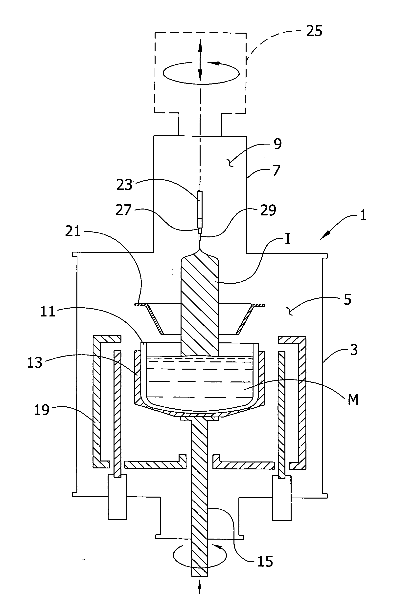
[0016] Referring to FIG. 1, a crystal pulling apparatus of one embodiment indicated generally at 1 is shown. The crystal pulling apparatus has a lower housing 3 enclosing a crystal growth chamber 5 and an upper housing 7 enclosing an upper pull chamber 9. The lower housing 3 enclosing the crystal growth chamber 5 houses a crystal growth crucible 11 seated in a susceptor 13. The crucible is suitably made of quartz and the susceptor of graphite, though other materials are contemplated. The crucible 11 contains molten source material M from which the monocrystalline silicon ingot I is grown. The susceptor 13 is mounted on a turntable 15 for rotation of the susceptor and crucible 11 about a central longitudinal axis of the crystal puller 1. The crucible 11 is also capable of being raised within the growth chamber 5 to maintain the surface of the molten source material M at a generally constant level as the ingot I is grown and source material is removed from the melt.

[0017] An electric...


PUM

PropertyMeasurementUnit
thickaaaaaaaaaa
thickaaaaaaaaaa
thicknessaaaaaaaaaa

Abstract

A crystal pulling apparatus for producing a silicon crystal ingot having a reduced amount of metal contamination. The apparatus includes a growth chamber and a component disposed within the growth chamber having a protective layer of silicon nitride for preventing metal contamination of the crystal.

Description

BACKGROUND OF THE INVENTION [0001] The present invention relates generally to an apparatus for the preparation of single silicon crystals having a reduced level of contamination. More specifically, the present invention relates to an apparatus for the preparation of single silicon crystals wherein a graphite component in a crystal growth chamber of a Czochralski crystal pulling apparatus has been coated with a protective layer of silicon nitride. [0002] Single crystal material having a monocrystalline structure, which is the starting material for fabricating many electronic components such as semiconductor devices and solar cells, is commonly prepared using the Czochralski (“Cz”) method. Briefly described, the Czochralski method involves melting polycrystalline source material such as granular or chunk polycrystalline silicon (“polysilicon”) in a quartz crucible located in a specially designed furnace to form a silicon melt. An inert gas such as argon is typically circulated through...

Claims


Application Information

Patent Timeline
Patent Type & Authority Applications(United States)
IPC IPC(8): C30B35/00C30B27/02C30B15/00C30B21/06C30B28/10C30B30/04
CPCC30B15/00Y10T117/1052C30B29/06C30B15/14
Inventor SREEDHARAMURTHY, HARIPRASADHOLDER, JOHN DAVISBANAN, MOHSEN
Owner MEMC ELECTONIC MATERIALS INC
Why Eureka
Try Eureka