On-chip igniter and method of manufacture

a technology of on-chip igniter and manufacturing method, which is applied in the direction of solid-state devices, weapons, semiconductor devices, etc., can solve the problems of large setup and cost, high cost, and high cost of available testing methods, and achieves small amount of combustible materials on any single device, easy and safe handling, and reasonable cost

Inactive Publication Date: 2007-05-03
UNIVERSITY OF MISSOURI
View PDF20 Cites 32 Cited by
  • Summary
  • Abstract
  • Description
  • Claims
  • Application Information

AI Technical Summary

Benefits of technology

[0014] The chip is inexpensive and can be built on the substrate less than 3 inches in size. Common materials are used in the manufacture of the chip, assuring the availability of the necessary components and maintaining a reasonable cost. No additional labor is needed to run complex equipment, such as high-speed digital cameras.
[0015] This apparatus also provides an easy and safe way of handling nanoenergetic materials. The amount of combustible material on any single device is very small, reducing the probability of damage if the nanoenergetic material is ignited by accident. Since the nanoenergetic material is fixed to the surface of the substrate, it is unlikely to spill or contaminate other products, and is much easier to handle compared to loose fine powders or particles.

Problems solved by technology

However, EBW devices, such as the tungsten bridge, when supplied with current, causes plasma to form which vaporizes the tungsten and causes the ignition of the energetic material.
Such setups are very large and expensive.
Available methods for testing are also expensive.
Testing devices that are unable to distinguish new products from each other are useless for screening new products.
Large-scale testing systems are not always available for investigation or rare, expensive or highly toxic statistical analysis or small labs on limited budgets.
These methods are very expensive and some require installation of high-speed digital imaging systems.
This method requires an oscilloscope or other expensive optical set up.
Each of these methods offers advantages but also significant limitations.
The light-ion-beam and radiation drivers generally do not permit rapid turn around.
Other characterization techniques use expensive high-speed movie cameras.
Moreover, these large-scale systems are impractical for investigation of rare, expensive or highly toxic materials.

Method used


Image

  • On-chip igniter and method of manufacture
  • On-chip igniter and method of manufacture
  • On-chip igniter and method of manufacture

Examples


example 1

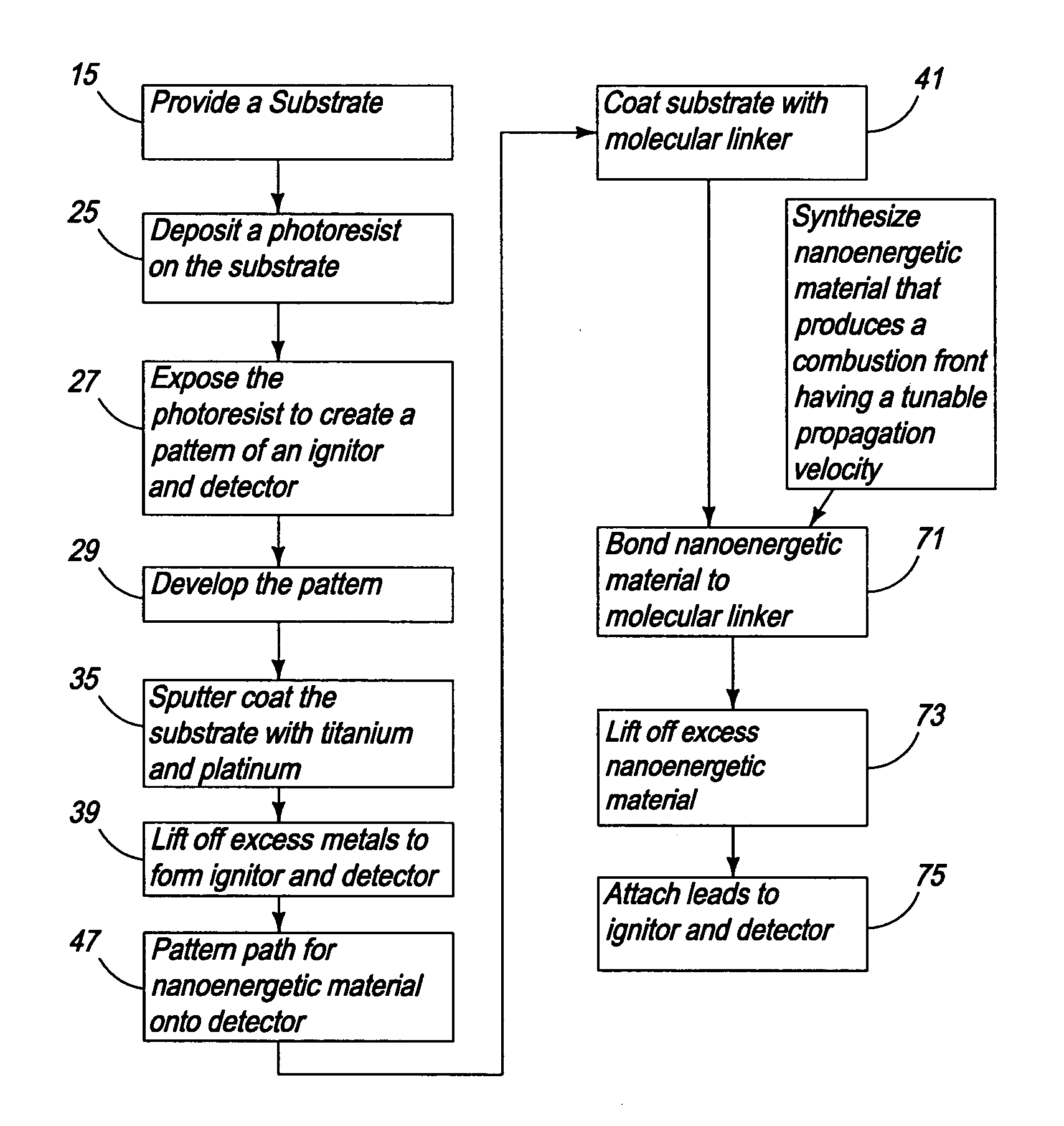
[0060] A diagnostic device was made on a glass substrate measuring 1 inch×3 inches (2.5 cm×7.5 cm). The glass was 0.035 inches thick. It was cleansed for ten minutes with Piranha solution consisting of sulfuric acid (H2SO4, 98%) and hydrogen peroxide (H2O2) in a 3:1 ratio. Residual acids and sulfates were removed from the substrate surface by rinsing the substrate in running distilled water. The cleaned substrate was dried at 105° C. for 15 minutes.

[0061] Shipley S1813 positive photoresist was spun onto the cleaned glass substrate at 650 rpm for 30 seconds and then oven dried at 110° C. for 7-8 minutes. A black and white transparency mask was printed at a resolution of 3200×3200 dots per inch with patterns for a heater and a time varying resistor. The substrate was then exposed to light in a Kienstein exposure tool for 105 seconds. Passage of light through the clear areas of the transparency allowed the photoresist to de-bond. The de-bonded resist was wet-etched from the substrate ...

example 2

[0066] Additional diagnostic apparatuses were made according to the method of Example 1, using different nanoenergetic materials. Bismuth oxide (Bi2O3) and aluminum nanoparticles were combined in a ratio of 70% oxidizer and 30% fuel, with a total weight of 1.37 g. The powders were dispersed in 5 mL of 2-propanol.

[0067] The flame propagation rate of the various nanoenergetic materials made by the process of Example 1 were measured using on-chip method. The chip was fabricated with the heater at one end and the time varying resistor at the other end by sputter coating the platinum film. This chip was coated with uniformly thick layer of nanoenergetic material and the chip was connected across a voltage divider circuit to measure the voltage drop across the time varying resistor detector film. The on-chip heater film was powered by a voltage supply which heated up the energetic material to its ignition point. Current of 2-3 Amps was supplied to the heater when ignition switch was togg...

example 3

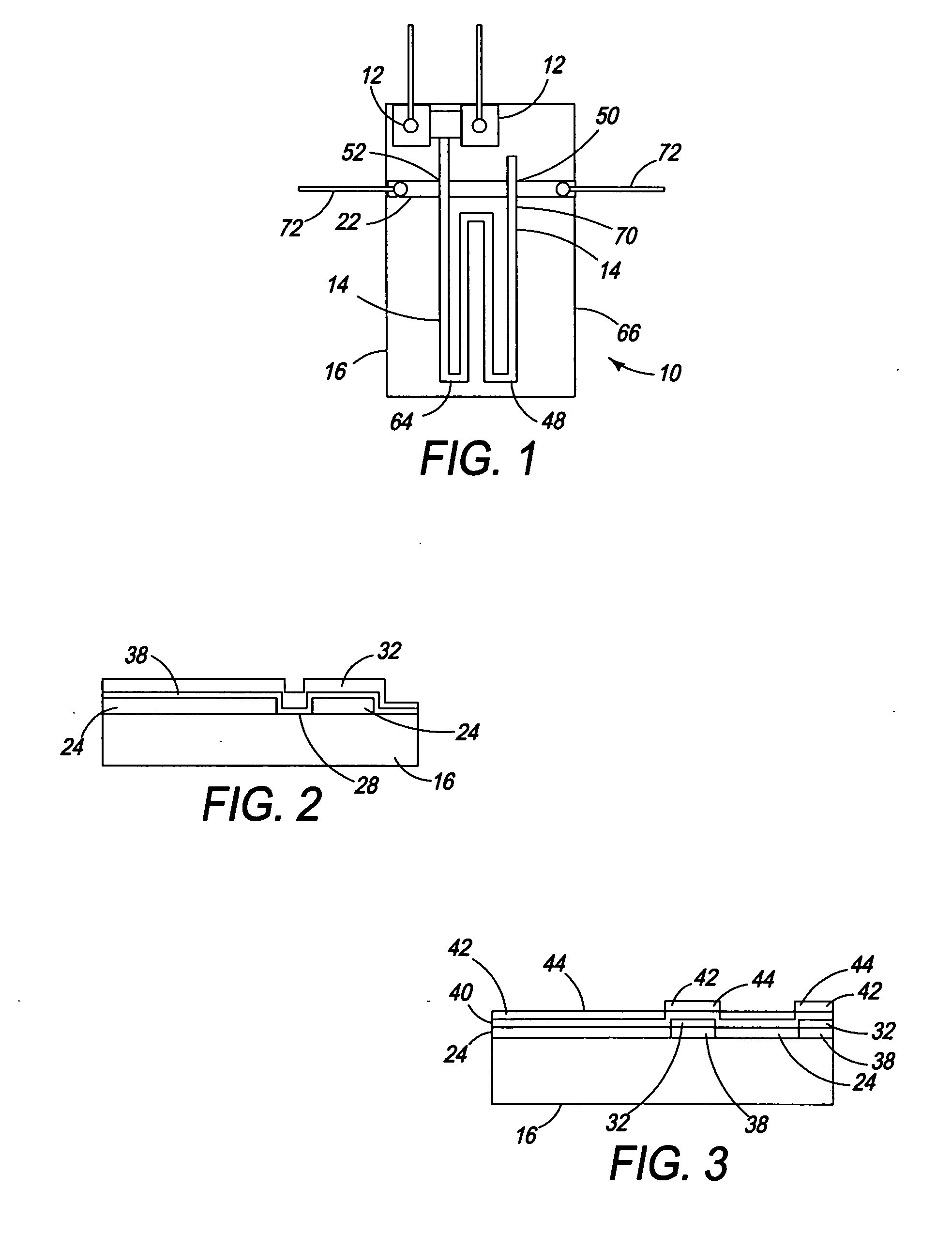
[0068] A multi-point Initiator apparatus was made using a microfabrication technique. Borofloat glass microscopic slides from (1×3 in.) were used as the substrate, which were cleaned using the procedure described in Example 1. The substrates were then shadow masked with aluminum (Al) foil in a square pattern of 5×5 mm. After masking the substrates, the sputtering process was performed. First, an interface layer, for adhesion promotion, of Ti was deposited about 10 nm thick. The sputtering system used for the prototypes called for sputtering the Ti at 150 mA for 1 min 50 sec to achieve the desired thickness. Then, the Pt film, about 650 nm thick, was deposited by sputtering 5 cycles at 90 mA for a total time of about 20 min (cycle time of 4 min each). This sputter-coating procedure produced about 130 nm thick films per cycle.

[0069] Once the films deposited, the shadow-mask was removed, and discarded. These glass substrates with a thin-film of Ti and Pt-layers were annealed in an ove...


PUM


Abstract

A chip for igniting nanoenergetic materials, includes a substrate, an igniter positioned on the substrate and the nanoenergetic material arranged in a linear pattern positioned on said substrate. A method of making a chip for igniting nanoenergetic materials includes providing a substrate, forming an igniter on the substrate and coating the substrate with a polymer layer. A pattern of nanoenergetic material comprising a fuel and an oxidizer is formed on the substrate. The nanoenergetic material is ignited by the igniter by supplying power to the leads attached to the heater film.

Description

CROSS REFERENCE TO RELATED APPLICATION [0001] This application is related to U.S. Ser. No. 11 / ___,___ (Attorney Docket No. 2114.73701), entitled, “Ordered Nanoenergetic Composites and Synthesis Method,” filed concurrently herewith and herein incorporated by reference.FIELD OF THE INVENTION [0002] This application relates to a chip for igniting nanoenergetic materials. More specifically, nanoenergetic materials are arranged in a pattern on the chip that includes an ingiter. The chip has many uses, including a diagnostic tool, a fuse, a power generator, a microthruster, detonators, igniter for explosives, igniter for propellans and for low temperature crystallization of thin films. BACKGROUND [0003] Nano-energetic materials are mixtures of fuel and oxidizers closely packed together for a self-sustaining, high temperature reaction. Tiny particles have increased surface area over larger particles. Close proximity of the fuel and the oxidizer create waves of energy as the flame propagate...

Claims


Application Information

Patent Timeline
Patent Type & Authority Applications(United States)
IPC IPC(8): H01L51/40
CPCF42B3/13
Inventor GANGOPADHYAY, SHUBHRASHENDE, RAJESHAPPERSON, STEVEBHATTACHARYA, SHANTANUGAO, YUANFANG
Owner UNIVERSITY OF MISSOURI
Why Eureka
Try Eureka