Organic electroluminescent device

a technology of electroluminescent devices and electroluminescent lamps, which is applied in the direction of discharge tubes/lamp details, luminescent screens for discharge tubes, natural mineral layered products, etc., can solve the problems of insufficient red purity, insufficient half life of luminance, and insufficient luminous efficiency and lifetime, etc., to achieve high efficiency, high color purity, and the effect of longer life of the devi

Inactive Publication Date: 2007-05-10
IDEMITSU KOSAN CO LTD
View PDF7 Cites 396 Cited by
  • Summary
  • Abstract
  • Description
  • Claims
  • Application Information

AI Technical Summary

Benefits of technology

[0043] As stated above, according to the invention, an organic EL device with a high efficiency can be obtained by selecting suitable compounds as materials for an electron-transporting layer and an emitting layer. The constitution of the invention enables an organic EL device with a high color purity in which the generation of excit

Problems solved by technology

However, its luminous efficiency and lifetime did not attain a practical level and were insufficient.
This luminescent device is excellent in red purity, but its applied voltage is as high as 11 V and the half life of luminance is as insufficient as about 150 hours.
Patent Document 5 discloses a device in which a dicyanomethylene (DCM) type co

Method used


Image

  • Organic electroluminescent device
  • Organic electroluminescent device
  • Organic electroluminescent device

Examples


example 1

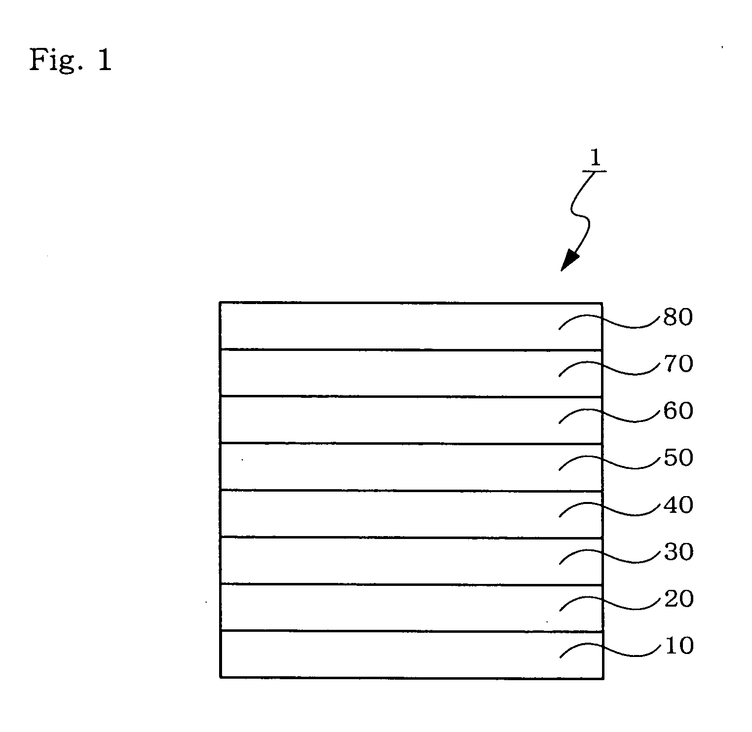
[0128] A 120 nm thick transparent electrode made of indium tin oxide was formed on a glass substrate measuring 25 mm×75 mm×0.7 mm. The glass substrate was subjected to ultrasonic cleaning in isopropyl alcohol for 5 minutes, and then subjected to UV ozone cleaning for 30 minutes. The glass substrate was placed in a vacuum deposition device.

[0129] First, as a hole-injection layer, N′,N″-bis[4-(diphenylamino)phenyl]-N′,N″-diphenylbiphenyl-4,4′-diamine was deposited to a thickness of 60 nm on the substrate. Then, as a hole-transporting layer, tetrakis-N-(4-biphenyl)benzidine was deposited to a thickness of 10 nm thereon. Next, as an emitting layer, the compound (A-1) of a naphthacene derivative below and the compound (B) of an indenoperylene derivative below were co-deposited to a thickness of 40 nm at a weight ratio of 40:0.4.

[0130] Next, as an electron-transporting layer, a compound (C-1) below was deposited to a thickness of 30 nm.

[0131] Next, a lithium fluoride was deposited to...

example 2

[0133] An organic EL device was fabricated in the same way as in Example 1 except that the compound (A-3) below of a diaminoanthracene derivative was used instead of the compound (A-1) when the emitting layer was formed.

[0134] When an electrical conduction test was performed for the device obtained, red emission with a driving voltage of 4.1 V and a luminance of 978 cd / m2 was obtained at a current density of 10 mA / cm2. Chromaticity coordinates were (0.67, 0.33), and a luminous efficiency was 9.78 cd / A. When a direct current continuous conduction test was performed at an initial luminance of 5,000 cd / m2, a half life was 2,000 hours.


PUM

PropertyMeasurementUnit
Fractionaaaaaaaaaa
Fractionaaaaaaaaaa
Energyaaaaaaaaaa

Abstract

An organic electroluminescent device 1 comprising, an emitting layer (50) and an electron-transporting layer (60) between a cathode (80) and an anode (20), the electron-transporting layer (60) comprising a compound represented by formula (1), the emitting layer (50) comprising a host material which is a compound with an energy gap of 2.8 eV or less represented by formula (2) and a dopant which is an indenoperylene derivative,
A-B   (1)
wherein A is an aromatic hydrocarbon group with three or more carbocycles and B is a substituted or unsubstituted heterocyclic group,
X—(Y)n   (2)
wherein X is a condensed aromatic ring group with three or more carbocycles, Y is a group selected from substituted or unsubstituted aryl, substituted or unsubstituted diarylamino, substituted or unsubstituted arylalkyl and substituted or unsubstituted alkyl groups, and n is an integer of 1 to 6, provided that Ys may be the same or different when n is 2 or more.

Description

TECHNICAL FIELD [0001] The invention relates to an organic electroluminescent device. In detail, it relates to an organic electroluminescent device having a long life time and a high luminous efficiency, and emitting red light. TECHNICAL BACKGROUND [0002] An organic EL device is a self-emission device by the use of the principle that a fluorescent compound emits light by the recombination energy of holes injected from an anode and electrons injected from a cathode when an electric field is impressed. [0003] Since C. W. Tang et al. of Eastman Kodak Co. reported a low-voltage driven organic EL device in the form of a stacked type device (C. W. Tang, S. A. Vanslyke, Applied Physics Letters, Vol. 51, p. 913, 1987, and the like) (Non-patent Document 1), studies on organic EL devices wherein organic materials are used as the constituent materials has actively conducted. [0004] Tang et al. uses tris(8-quinolinol)aluminum for an emitting layer and a triphenyldiamine derivative for a hole-tr...

Claims


Application Information

Patent Timeline
IPC IPC(8): H01L51/54
CPCH01L51/0054H01L51/0056H01L51/0058H01L51/5048H01L51/0072H01L51/5012H01L51/006H10K85/624H10K85/622H10K85/626H10K85/633H10K85/6572H10K50/14H10K50/11H10K2101/90
Inventor ARAKANE, TAKASHIKUMA, HITOSHIFUKUOKA, KENICHIYAMAMOTO, HIROSHIHOSOKAWA, CHISHIO
Owner IDEMITSU KOSAN CO LTD
Why Eureka
Try Eureka