Ferroelectric memory device

a memory device and ferroelectric technology, applied in the direction of solid-state devices, vacuum evaporation coatings, coatings, etc., can solve the problems of difficult material orientation control, difficult composition control of pb, deterioration of the environment, etc., and achieve high ferroelectric characteristic, high dielectric polarization moment, and high performance

Inactive Publication Date: 2007-05-17
SEIKO EPSON CORP
View PDF5 Cites 16 Cited by
  • Summary
  • Abstract
  • Description
  • Claims
  • Application Information

AI Technical Summary

Benefits of technology

[0014] In order to resolve the above-described problem, the present invention provides a ferroelectric memory device including an Si oxide film, an electrode made of a perovskite material and formed on the Si oxide film, and a (001)-oriented BiFeO3 ferroelectric layer with a tetragonal structure formed on the electrode. According to this ferroelectric memory device, it is possible to directly mount a ferroelectric memory device including a ferroelectric layer onto an Si substrate because a BiFeO3 ferroelectric layer can grow epitaxially on an electrode made of a perovskite material (material having a perovskite structure) formed on an Si oxide film. The ferroelectric memory device has a (001)-oriented BiFeO3 layer with a tetragonal structure as a ferroelectric layer, which has a high ferroelectric characteristic such as a high dielectric polarization moment, and therefore the memory device has a high performance and is environmentally preferable because of no inclusion of Pb therein.
[0015] In the ferroelectric memory device, it is preferable that the electrode made of a perovskite or perovskite-type material be formed by an ion beam assist deposition method. According to this ferroelectric memory device, the electrode made of a perovskite-type material can grow epitaxially with ease, for example, on a natural oxide film on an Si substrate.
[0016] In the ferroelectric memory device, it is preferable that the electrode made of a perovskite-type material be epitaxially grown with a (100)-orientation. According to this ferroelectric memory device, a (001)-oriented BiFeO3 ferroelectric layer with a tetragonal structure can grow epitaxially with good quality on the electrodes.

Problems solved by technology

However, composition control of Pb is difficult because Pb can easily evaporate from the ferroelectric layers.
Additionally, the evaporation of Pb leads to deterioration of the environment because Pb is harmful thereto.
However, its orientation control in the materials is difficult because of a layered structure, and miniaturization of devices made of these materials is difficult because of the existence of crystal grains in the materials.
Additionally, the materials are damaged by hydrogen at the time of formation of a passivation film in a post-process.
Since BaTiO3 has such a transition temperature near the operating temperature, the value of the dielectric polarization moment is unstable and the materials may degrade easily with the structural phase transition.
However, there is a problem to be solved in a ferroelectric memory device using BiFeO3, that is, it is very difficult to directly implement the ferroelectric memory device including a lower electrode on an Si substrate.
This is because normally a natural oxide film is formed on an Si substrate, and it is difficult to make a lower electrode film and a BiFeO3 film grow epitaxially on the natural oxide film.

Method used


Image

  • Ferroelectric memory device
  • Ferroelectric memory device
  • Ferroelectric memory device

Examples


Embodiment Construction

[0039] Hereinafter, ferroelectric memory devices of the present invention are described in detail.

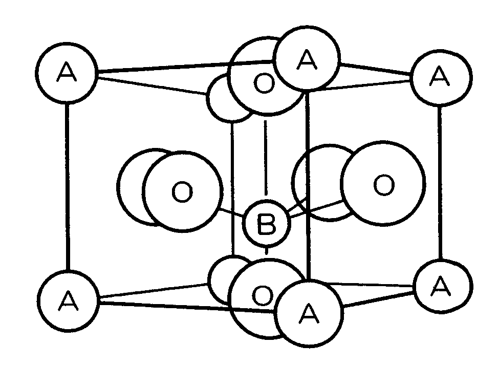
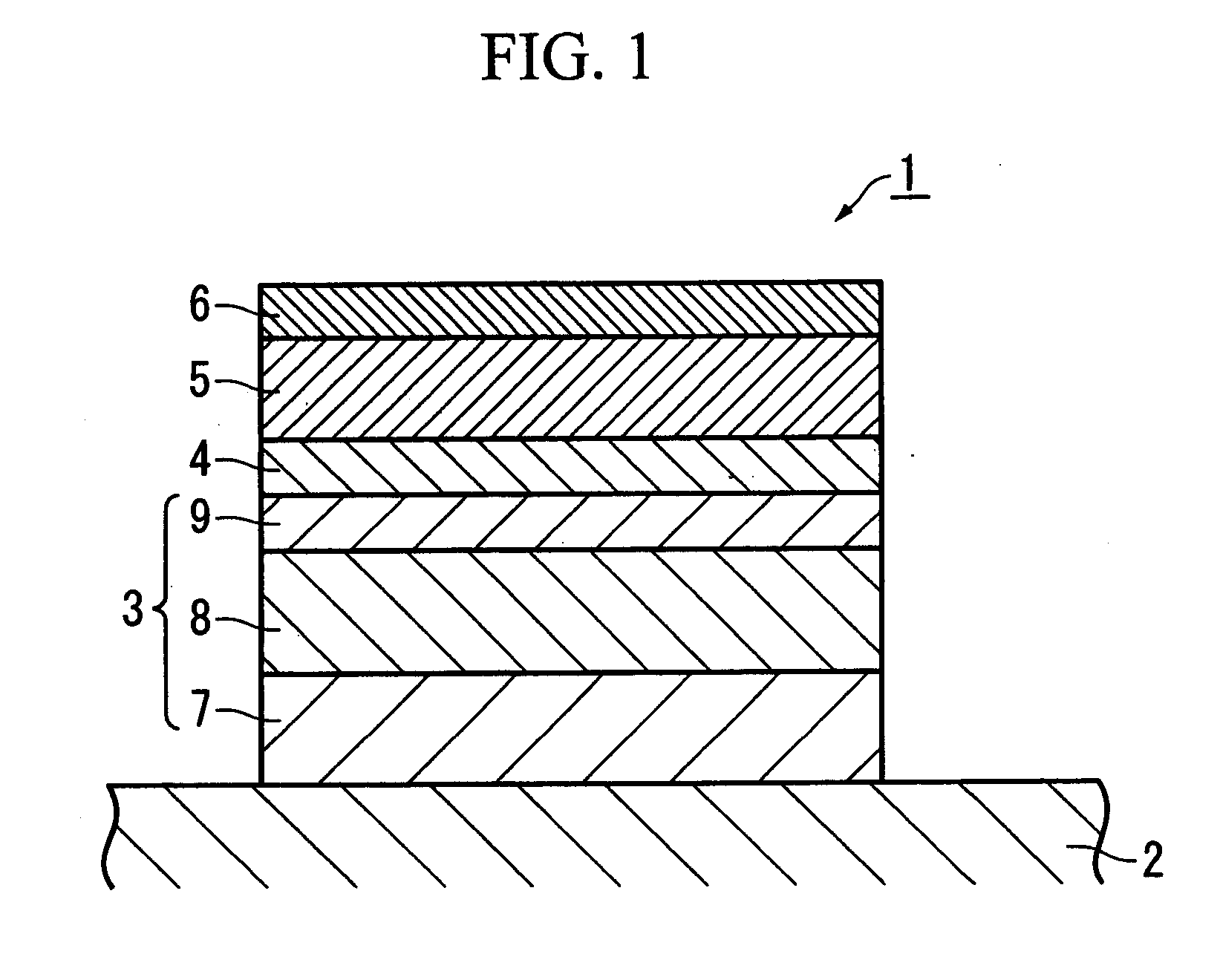
[0040]FIG. 1 shows a schematic illustration of an embodiment of a ferroelectric memory device of the present invention, where reference number 1 shows a ferroelectric memory device. The ferroelectric memory device 1 is formed on a (100)-plane of a silicon (Si) substrate 2, and includes a buffer layer 3 formed on the Si substrate 2, a lower electrode 4 formed on the buffer layer 3, a ferroelectric layer 5 formed on the lower electrode 4, and an upper electrode 6 formed on the ferroelectric layer 5.

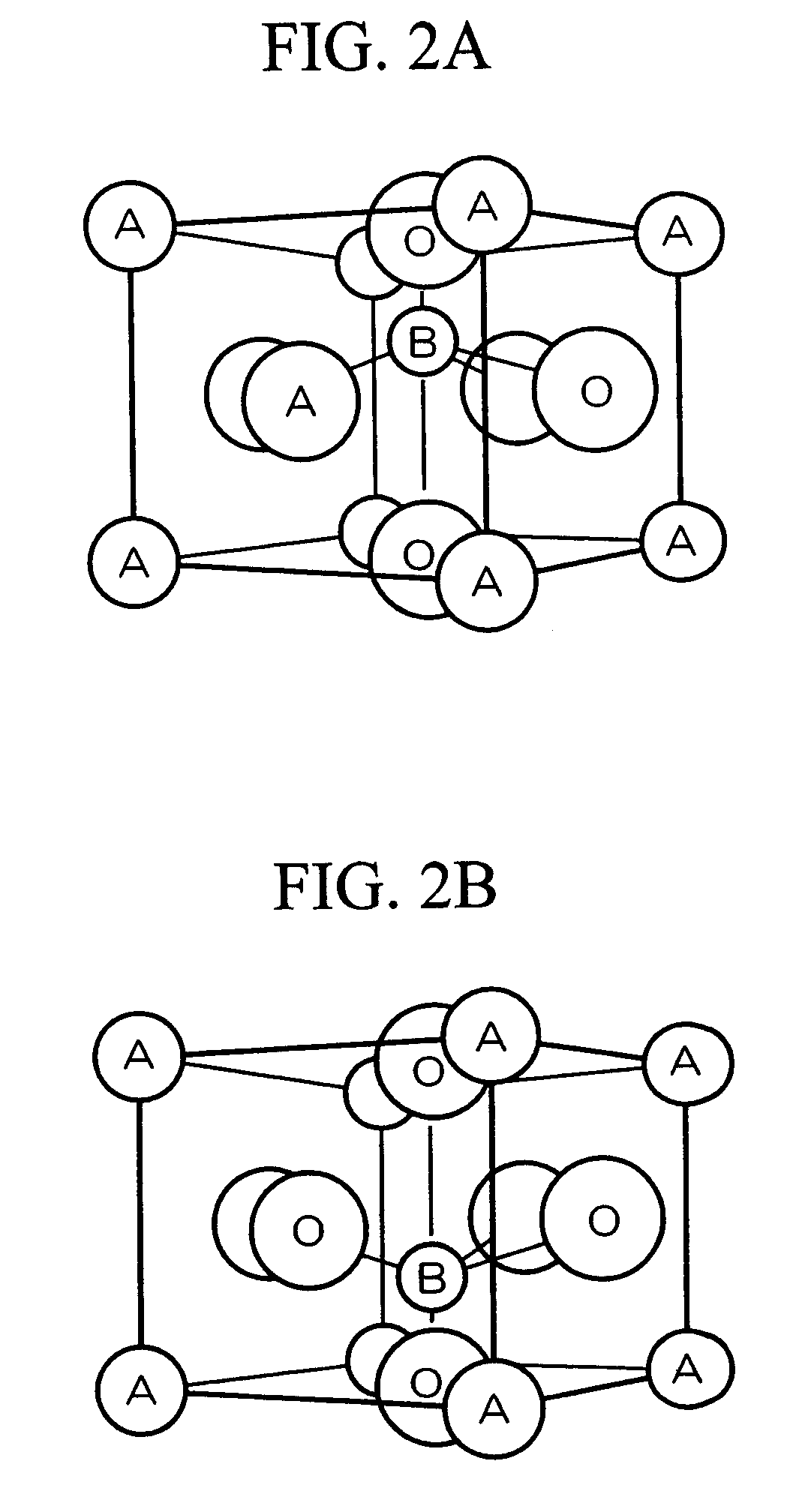
[0041] A layer formed of grains with a single orientation, i.e., only with an orientation parallel to the through-thickness of a layer, can be used as the buffer layer 3, and it is preferable that the grains in the buffer layer also have a planer orientation, i.e., the grains have orientations in all three-dimensions. This is because good bonding or adhesion between the Si substrate 2 with a ...


PUM

PropertyMeasurementUnit
Curie temperatureaaaaaaaaaa

Abstract

A ferroelectric memory device has a high performance, includes no Pb, and can be directly mounted onto an Si substrate. The ferroelectric memory device includes a (001)-oriented BiFeO3 ferroelectric layer 5 with a tetragonal structure, which is formed on an electrode 4 made of a perovskite material formed on an Si oxide film. The electrode 4 with a perovskite structure is formed by an ion beam assist method.

Description

[0001] This is a Division of Application of U.S. patent application Ser. No. 10 / 867,812, filed Jun. 16, 2004. The entire disclosure of the prior application is hereby incorporated by reference herein in its entirety.BACKGROUND OF THE INVENTION [0002] 1. Field of the Invention [0003] This invention relates to a ferroelectric memory device including a BiFeO3 ferroelectric layer. [0004] Priority is claimed on Japanese Patent Application No. 2003-173247, filed Jun. 18, 2003, the content of which is incorporated herein by reference. [0005] 2. Description of Related Art [0006] Ferroelectric materials are beginning to be put to practical use as recording materials in nonvolatile memory devices because they have a large capacity and low power consumption. Pb(Zr1-xTux)O3 (PZT) which is a perovskite-type oxide and SrBi2Ta2O9 (SBT) which is a Bi layered compound are representatives of ferroelectric materials used in nonvolatile memory devices. For a nonvolatile memory device using such ferroel...

Claims


Application Information

Patent Timeline
Patent Type & Authority Applications(United States)
IPC IPC(8): H01L21/00H01L29/94H01L29/76C23C14/08C23C14/22H01L21/316H01L21/8246H01L27/105H01L27/115H01L31/109
CPCH01L21/31691H01L27/11502H01L27/11507H01L28/55H01L21/02197H10B53/30H10B53/00
Inventor MIYAZAWA, HIROMUHIGUCHI, TAKAMITSUIWASHITA, SETSUYA
Owner SEIKO EPSON CORP
Why Eureka
Try Eureka