Sequential Selective Epitaxial Growth

Active Publication Date: 2007-05-31
SYNOPSYS INC
View PDF3 Cites 366 Cited by
  • Summary
  • Abstract
  • Description
  • Claims
  • Application Information

AI Technical Summary

Benefits of technology

[0011] Conventional metal-oxide-semiconductor field effect transistor (MOSFET) designs face significant challenges as they are scaled down to improve cost and/or performance with each new generation of technology used to manufacture integrated circuits (ICs). In particular, the techniques used to reduce static power consumption by minimizing source-to-drain leakage current (e.g., increased channel doping, decreased gate-dielectric thickness, and decreased source and drain junction depths) tend to also decrease transi

Problems solved by technology

Conventional metal-oxide-semiconductor field effect transistor (MOSFET) designs face significant challenges as they are scaled down to improve cost and/or performance with each new generation of technology used to manufacture integrated circuits (ICs).
In particular, the techniq

Method used


Image

  • Sequential Selective Epitaxial Growth
  • Sequential Selective Epitaxial Growth
  • Sequential Selective Epitaxial Growth

Examples


Embodiment Construction

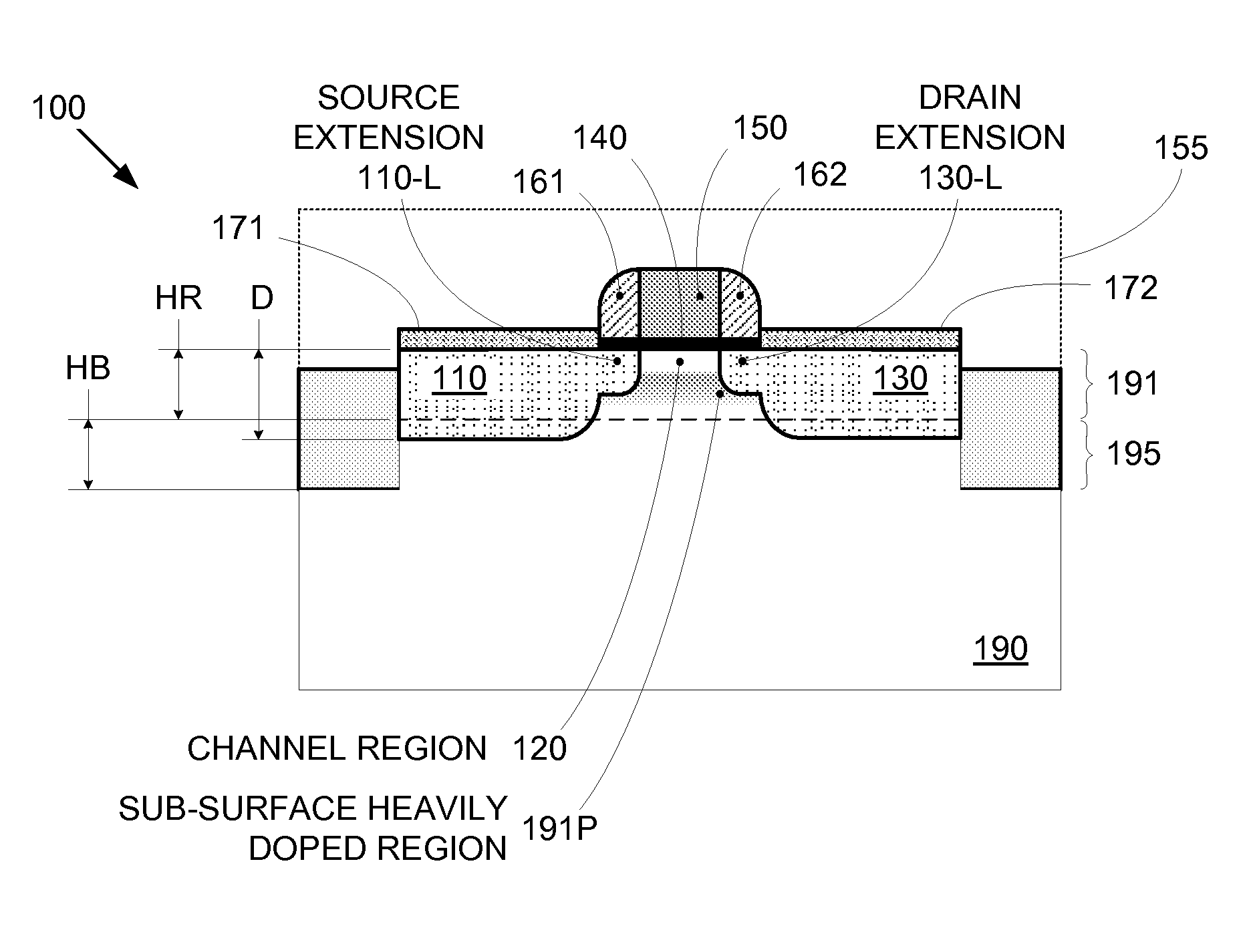
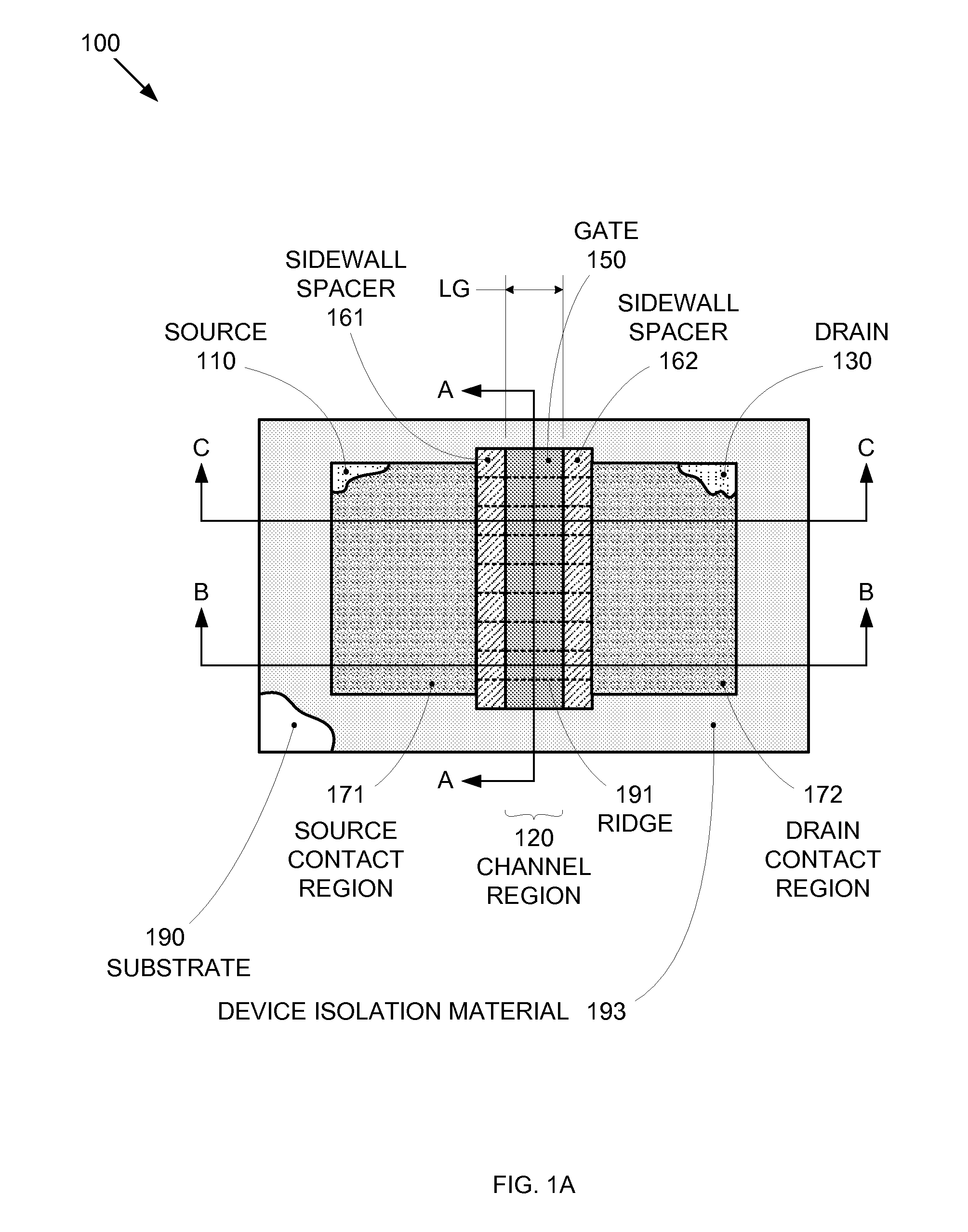
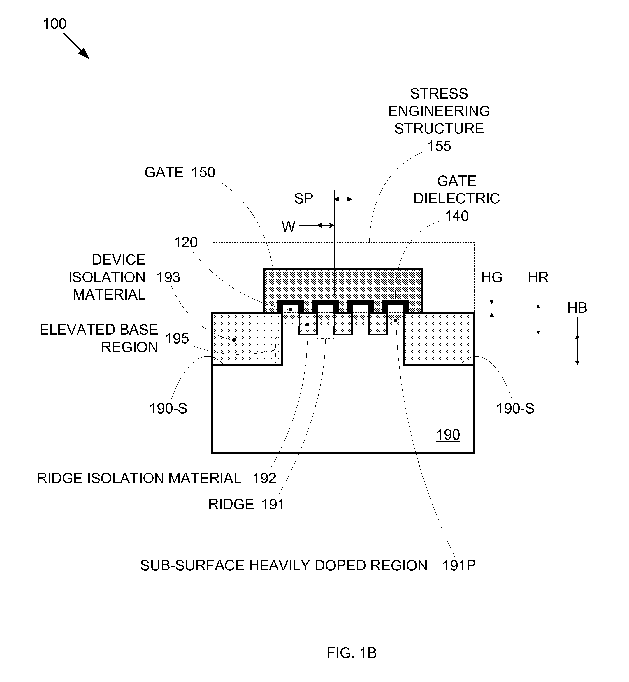
[0025] Conventional metal-oxide-semiconductor field effect transistor (MOSFET) designs face significant problems as those designs are scaled down to improve the cost and performance of integrated circuits (ICs). In particular, the techniques used to reduce static power consumption by minimizing source-to-drain leakage current (e.g., increased channel doping, decreased gate-dielectric thickness, decreased source and drain junction depths) tend to also decrease transistor performance by decreasing on-current. By forming MOSFETs over a substrate having precisely-formed stripes (ridges of semiconductor material(s)), both high performance (i.e., high on-current) and low static power consumption (i.e., low source-to-drain leakage current) can be achieved with good uniformity. The stripes enable the formation of segmented channel regions that accommodate a wide range of gate-electrode configuration options and also provide greater performance consistency between devices.

[0026]FIG. 1A show...


PUM


Abstract

By forming MOSFETs on a substrate having pre-existing ridges of semiconductor material (i.e., a “corrugated substrate”), the resolution limitations associated with conventional semiconductor manufacturing processes can be overcome, and high-performance, low-power transistors can be reliably and repeatably produced. Forming a corrugated substrate prior to actual device formation allows the ridges on the corrugated substrate to be created using high precision techniques that are not ordinarily suitable for device production. MOSFETs that subsequently incorporate the high-precision ridges into their channel regions will typically exhibit much more precise and less variable performance than similar MOSFETs formed using optical lithography-based techniques that cannot provide the same degree of patterning accuracy. A multi step epitaxial process can be used to extend the ridges with different dopant types, high mobility semiconductor, and or advanced multi-layer strutures. For CMOS integrated circuits a capping layer is formed over the a first region. Epitaxial layers are formed in a second region. Then the capping layer is removed from the first region and a capping layer is formed over the second region. Epitaxial layers can than be formed in the first region.

Description

RELATED APPLICATIONS [0001] The present application is a Continuation-In-Part of and claims the benefit of U.S. Utility patent application Ser. No. 11 / 173,237 by Tsu-Jae King et al., filed Jul. 1, 2005, and is incorporated herein in its entirety by reference.BACKGROUND OF THE INVENTION [0002] 1. Field of the Invention [0003] The invention relates to the field of semiconductor integrated-circuit devices and manufacturing, and in particular to structures for enhancing miniature transistor manufacturability and performance. [0004] 2. Related Art [0005] Semiconductor integrated-circuit (IC) manufacturers face growing challenges to accurately and reliably produce ever-smaller transistors in order to improve the cost and performance (speed and / or functionality) of modern electronic devices. The most basic building block used in a digital IC device is the metal-oxide-semiconductor field effect transistor (MOSFET). As MOSFETs are scaled below 100 nm in minimum lateral dimension (i.e., the m...

Claims


Application Information

Patent Timeline
IPC IPC(8): H01L21/337
CPCH01L21/823807H01L21/823821H01L27/0207H01L29/66795H01L29/785
Inventor LIU, TSU-JAE KINGLU, QIANG
Owner SYNOPSYS INC
Why Eureka
Try Eureka