

Method of producing thin films
a technology of thin films and nitride, which is applied in the field of thin films, can solve the problems that the silicon or boron doping of ald nitride thin films is not known in the art, and achieve the effects of reducing the work function of metal gates, reducing the crystallinity of films, and reducing the crystallinity
- Summary
- Abstract
- Description
- Claims
- Application Information
AI Technical Summary
Benefits of technology
Problems solved by technology
Method used
Image

Examples
example 1
[0125] ALD hafnium oxide thin films deposited on native silicon oxide were used as a substrates for NbN and Nb(Si)N deposition. Substrates were loaded in an ASM F-120™ reactor.
[0126] NbN film was deposited by ALD from NbCl5 and NH3. Nb(Si)N film was deposited by ALD with a pulsing ratio of 5:1 metal nitride cycles to cycles including the Si dopant, from NbCl5, SiCl4 and NH3 precursors (i.e. where n=5 and m=1 and k=100 in the equation presented above). Table 1 shows the rest of both deposition process parameters. Films deposited with these parameters were repeatable and uniform with low impurity contents (impurity levels that are typical for this kind of research reactor).
TABLE 1Parameters of ALD NbN and Nb(Si)N process.ParameterParameter valueReaction temperature400° C.NbCl5 pulse0.5 sNbCl5 purge2.0 sNbCl5 temperature90° C.NH3 pulse1.0 sNH3 purge3.0 sNH3 flow rate˜40 sccmSiCl4 pulse0.5 sSiCl4 purge5.0 sSiCl4 flow rateroughly 20 sccmNH3 pulse (after SiCl4)5.0 sNH3 purge (after SiC...
example 2
[0129] NbN and Nb(Si)N layers were deposited in an F-450 ALCVD™ reactor. Full size 200 mm silicon wafers were used in as substrates. Deposition was carried out at 400° C. either on a thick HfO2 film (40-70 nm) or on native or thermal SiO2. A source temperature of 75-95° C. was used for the NbCl5 reactant.
[0130] A growth rate of 0.3 Å / cycle was obtained for NbN on 200 mm wafers in the F-450 reactor. The average film thickness and uniformity on 200 mm wafers stayed nearly constant in spite of the change in the NbCl5 dose, indicating the self-limiting (ALD) nature of the growth (see FIG. 4). Roughness and density of 12.5 nm (or 500 cycles) NbN film were determined by XRR to be 2 nm and 8.21 g / cm3, respectively. ALD deposited NbN had a density of 8.21 g / cm3, which is very close to the bulk NbN density of 8.47 g / cm3.
[0131] The growth rate of Nb(Si)N on 200 mm wafers with a pulsing ratio of Nb:Si of 5:1 (i.e., silicon is introduced in every fifth cycle) was 0.34 Å / cycle at 400° C. Bonds...
example 3
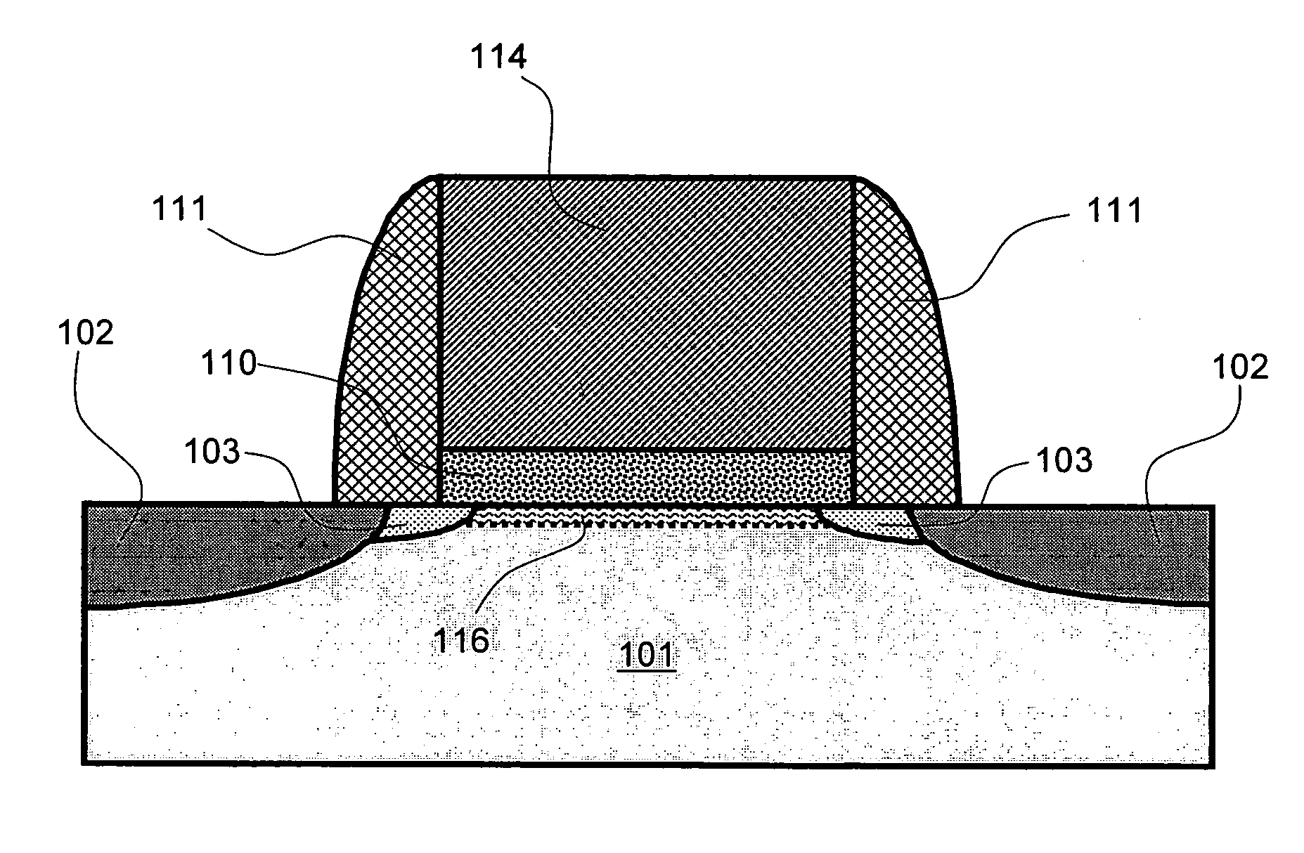
[0133] A hafnium oxide gate dielectric layer is deposited by ALD on a very thin layer of silicon oxide, which has itself been deposited or formed on a substrate by any appropriate method. The silicon oxide on the semiconductor substrate ensures that the initiation of the growth of hafnium oxide by ALD is favorable (i.e. there are enough active surface sites, such as —OHx-groups, on the surface of the substrate). A desired thickness of hafnium oxide is deposited by ALD using HfCl4 and H2O as precursors at a deposition temperature of about 300° C. Nitrogen is used as a carrier gas and a purging gas. Preferably HfCl4 is introduced to the reaction chamber as the first precursor in the first deposition cycle. Preferably H2O is introduced as the last precursor of the last deposition cycle, in order to provide more active surface sites on the surface of the deposited HfO2.
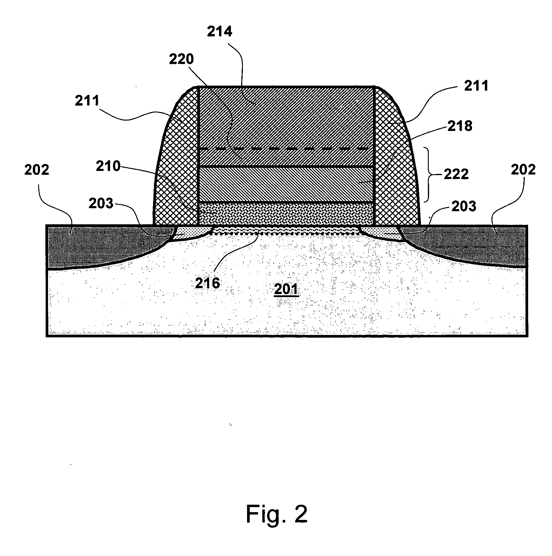
[0134] A niobium silicon nitride film is deposited over the HfO2 film. The niobium silicon nitride film is preferably ...
PUM
| Property | Measurement | Unit |
|---|---|---|
| temperature | aaaaa | aaaaa |
| temperatures | aaaaa | aaaaa |
| resistivities | aaaaa | aaaaa |
Abstract
Description
Claims
Application Information