Organic insulator composition, organic insulating film having the same, organic thin film transistor having the same and electronic device having the same and methods of forming the same

a technology of organic insulating film and organic insulating film, which is applied in the direction of liquid organic insulators, organic chemistry, transportation and packaging, etc., can solve the problems of insufficient insulating film replacement of inorganic insulating film, inability to use plastic substrates suitable for flexible display manufacturing, and inability to use common wet processes to fabricate devices. , to achieve the effect of improving the mobility and hysteria of the charge carrier of the organic thin

Active Publication Date: 2007-06-07
SAMSUNG ELECTRONICS CO LTD
View PDF6 Cites 22 Cited by
  • Summary
  • Abstract
  • Description
  • Claims
  • Application Information

AI Technical Summary

Benefits of technology

[0003] Example embodiments of the present invention relate to an organic insulator composition, an organic insulating film having the organic insulator composition, an organic thin film transistor having the organic insulator composition, an electronic device having the organic thin film transistor and methods of forming the same. Other example embodiments of the present invention relate to an organic insulator composition including a fluorinated silane compound that may be used to improve the charge carrier mobility and hysteresis of an organic thin film transistor.

Problems solved by technology

Because most fabrication processes require a relatively high temperature of about 200° C.˜about 400° C., plastic substrates suitable for use in the manufacture of flexible displays may not be used.
Common wet processes (e.g., simple coating and / or printing) may not be applied to fabricate the devices.
The characteristics of organic insulating films formed using the materials may be insufficient to replace inorganic insulating films.

Method used


Image

  • Organic insulator composition, organic insulating film having the same, organic thin film transistor having the same and electronic device having the same and methods of forming the same
  • Organic insulator composition, organic insulating film having the same, organic thin film transistor having the same and electronic device having the same and methods of forming the same
  • Organic insulator composition, organic insulating film having the same, organic thin film transistor having the same and electronic device having the same and methods of forming the same

Examples


synthesis example 1

Synthesis of Silane Compound A

[0078]

[0079] About 436.5 g (about 2.0 mol) of (3,3,3,-trifluoropropyl)trimethoxysilane was put in a one-liter reactor under a nitrogen atmosphere and cooled to about −30° C. About 6 ml (about 0.006 mol) of about 1.0N HCI and about 354 ml (about 199.99 mol) of distilled water were charged into a dropping funnel and installed on the reactor. As the reaction solution was cooled, about 360 ml of the aqueous HCI solution was added dropwise thereto. After completion of the addition, the reaction solution was stirred at about room temperature for about 3 hours. The reaction solution was poured into a separatory funnel and then about 1,000 ml of ethyl acetate and about 1,000 ml of water were added thereto to obtain an organic layer. About 10 g of sodium sulfate was added to the organic layer, stirred for about 2 hours, filtered, and evaporated to remove the solvents. The result was the desired silane compound A (weight-average molecular weight: about 19,000) a...

synthesis example 2

Synthesis of Silane Compound B

[0081]

[0082] About 447.05 g (about 1.8 mol) of 3-(trimethoxysilyl)propyl methacrylate and about 43.65 g (about 0.2 mol) of (3,3,3,-trifluoropropyl)trimethoxysilane were put in a one-liter reactor under a nitrogen atmosphere and cooled to about −30° C. About 6 ml (about 0.006 mol) of about 1.0N HCI and about 354 ml (about 199.99 mol) of distilled water were charged into a dropping funnel and installed on the reactor. As the reaction solution was cooled, about 360 ml of the aqueous HCI solution was added dropwise thereto. After completion of the addition, the reaction solution was stirred at about room temperature for about 3 hours. The reaction solution was poured into a separatory funnel, and then, about 1,000 ml of ethyl acetate and about 1,000 ml of water were added thereto to obtain an organic layer. About 10 g of sodium sulfate was added to the organic layer, stirred for about 2 hours, filtered, and evaporated to remove the solvents. The result was...

example 1

Fabrication of Bottom-contact Pentacene TFT

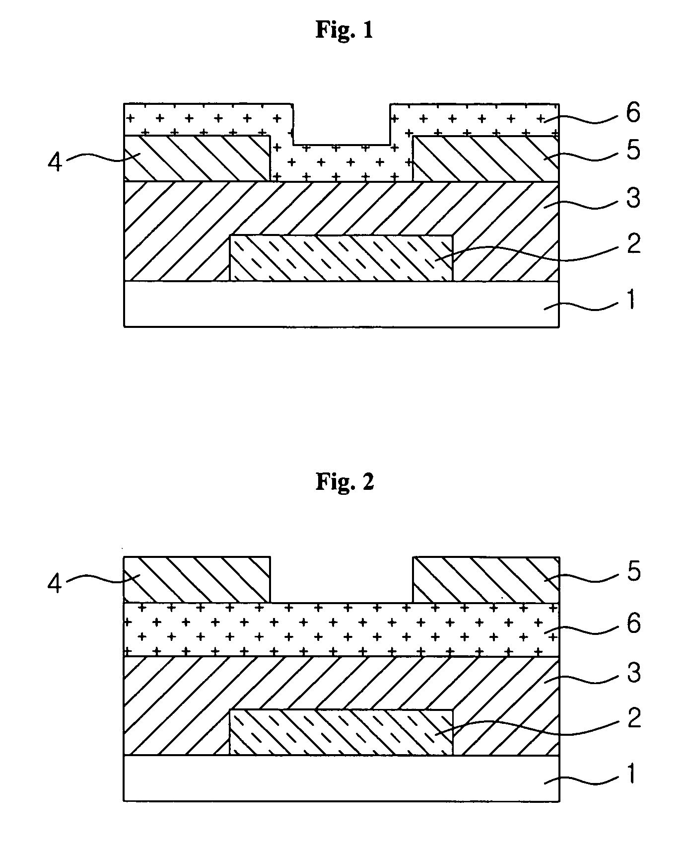
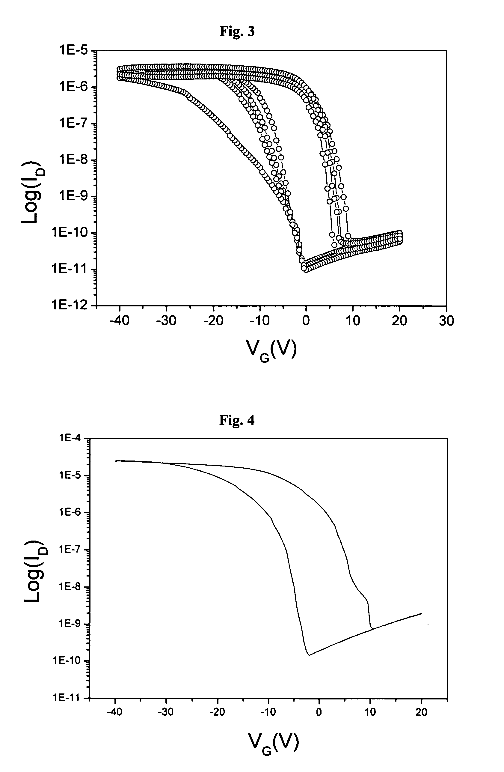
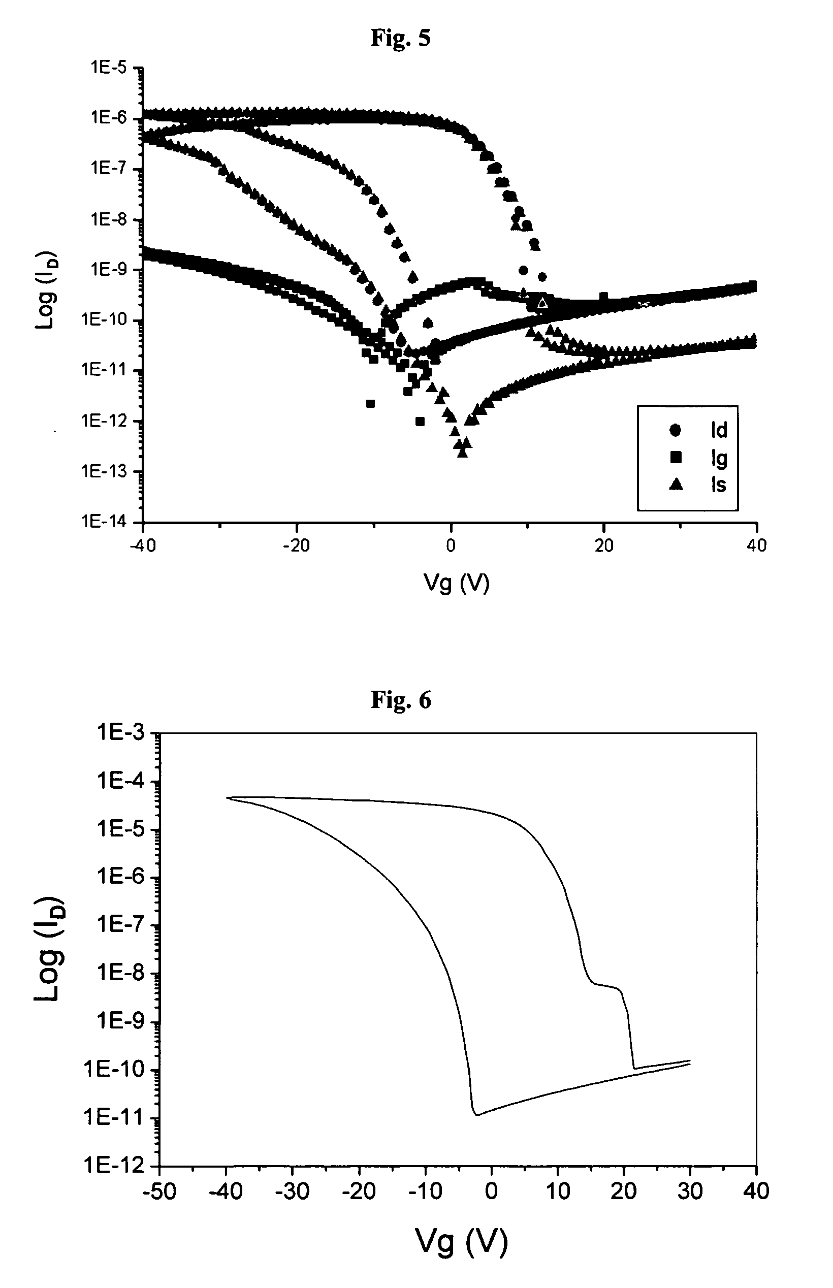
[0085] Aluminum was deposited on a clean glass substrate to form an about 800 Å-thick gate electrode. Thereafter, the organic insulator composition prepared in Preparative Example 2 was spin-coated to a thickness of about 8,000 Å thereon at about 2,000 rpm and baked at about 100° C. for about one hour to form an organic insulating film. About 500 Å-thick sourceldrain ITO electrodes (channel length: about 100 μm, channel width: about 1 mm) were formed on the organic insulating film and pentacene was deposited to a thickness of about 700 Å thereon by organic molecular beam deposition (OMBD) to form an organic semiconductor layer, completing the fabrication of a bottom-contact organic thin film transistor. The structure of the transistor is illustrated in FIG. 1.


PUM

PropertyMeasurementUnit
temperatureaaaaaaaaaa
dielectric constantaaaaaaaaaa

Abstract

Example embodiments of the present invention relate to an organic insulator composition, an organic insulating film having the organic insulator composition, an organic thin film transistor having the organic insulating film, an electronic device having the organic thin film transistor and methods of forming the same. Other example embodiments of the present invention relate to an organic insulator composition including a fluorinated silane compound that may be used to improve the charge carrier mobility and hysteresis of an organic thin film transistor. An organic insulator composition including a fluorinated silane compound and an organic thin film transistor using the same is provided. The hysteresis and physical properties, e.g., threshold voltage and/or charge carrier mobility, of the organic thin film transistor may be improved by the use of the organic insulator composition. The organic thin film transistor may be effectively used in the manufacture of a variety of electronic devices including liquid crystal displays (LCDs) and/or photovoltaic devices.

Description

PRIORITY STATEMENT [0001] This non-provisional application claims priority under 35 U.S.C. § 119(a) to Korean Patent Application No. 2005-117964, filed on Dec. 6, 2005, in the Korean lntellectual Property Office (KIPO), the entire contents of which are herein incorporated by reference. BACKGROUND [0002] 1. Field [0003] Example embodiments of the present invention relate to an organic insulator composition, an organic insulating film having the organic insulator composition, an organic thin film transistor having the organic insulator composition, an electronic device having the organic thin film transistor and methods of forming the same. Other example embodiments of the present invention relate to an organic insulator composition including a fluorinated silane compound that may be used to improve the charge carrier mobility and hysteresis of an organic thin film transistor. [0004] 2. Description of the Related Art [0005] Flat panel displays (e.g., liquid crystal displays and / or org...

Claims


Application Information

Patent Timeline
Patent Type & Authority Applications(United States)
IPC IPC(8): C04B41/50B60C1/00
CPCH01L21/3122H01L51/0036H01L51/0055H01L51/052Y10T428/31663H01L21/02126H01L21/02175H10K85/113H10K85/623H10K10/471H01B3/22H01B3/24
Inventor SHIN, JUNG HANLEE, EUN KYUNGJEONG, EUN JEONGKIM, JOO YOUNGMOON, HYUN SIKLEE, SANG YOON
Owner SAMSUNG ELECTRONICS CO LTD
Why Eureka
Try Eureka