Semiconductor device and method of fabricating the same background

a semiconductor and background technology, applied in the field of semiconductor devices, can solve the problems of inferior transistor characteristics of field effect transistors formed in such silicon thin films, grain boundaries of silicon thin films formed on insulating films, and flatness of base insulating films, so as to prevent deterioration of carrier mobility, stabilize transistor characteristics, and suppress crystallinity deterioration

Inactive Publication Date: 2007-06-14
SEIKO EPSON CORP
View PDF5 Cites 17 Cited by
  • Summary
  • Abstract
  • Description
  • Claims
  • Application Information

AI Technical Summary

Benefits of technology

[0009] An advantage of the present invention is to provide a semiconductor and a method of manufacturing the same that can suppress deterioration of crystallinity of a semiconductor layer having a field effect transistor formed therein, prevent deterioration of the carrier mobility regardless of whether the threshold voltage is high or low, and achieve a stable transistor characteristic, or can improve dynamic threshold controllability by a back gate electrode.
[0010] A semiconductor device according to a first aspect of the invention includes a semiconductor layer formed on a semiconductor substrate by epitaxial growth, a first embedded insulating layer embedded in a first region between the semiconductor substrate and the substrate layer, and a second embedded insulating layer embedded in a second region between the semiconductor substrate and the semiconductor layer, wherein the first embedded insulating layer and the second embedded insulating layer are mutually different in at least either one of effective work function and fixed charge amount.
[0011] According to this aspect, even when the body region of the semiconductor layer is doped intrinsically or in a low concentration, it is possible to mix field effect transistors with different threshold voltages on the same substrate. Since it is possible to lower the dopant concentration of the semiconductor layer regardless of whether the threshold voltage is high or low, even when field effect transistors with different threshold voltages are mixed on the same substrate, it is possible to improve the carrier mobility of all the mixed field effect transistors and thus to increase the on-current. Further, since it is possible to lower the impurity concentration of the substrate layer insofar as the shor

Problems solved by technology

However, the silicon thin film formed on the insulating film has grain boundaries, microtwins, and other various minute faults.
This has resulted in a problem that a field effect transistor formed in such a silicon thin film is inferior in transistor characteristic to a field effect transistor formed in a perfect single-crystal silicon.
This has caused a problem that flatness of a base insulating film, in which an upper layer silicon thin film is formed, is deteriorated.
This has also caused a problem that due to a limitation imposed on the thermal treatment conditions and t

Method used


Image

  • Semiconductor device and method of fabricating the same background
  • Semiconductor device and method of fabricating the same background
  • Semiconductor device and method of fabricating the same background

Examples


first embodiment

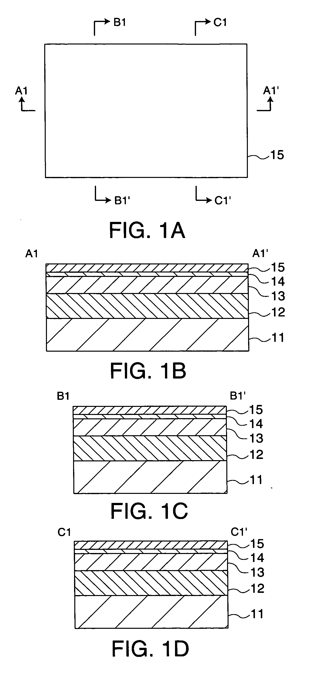
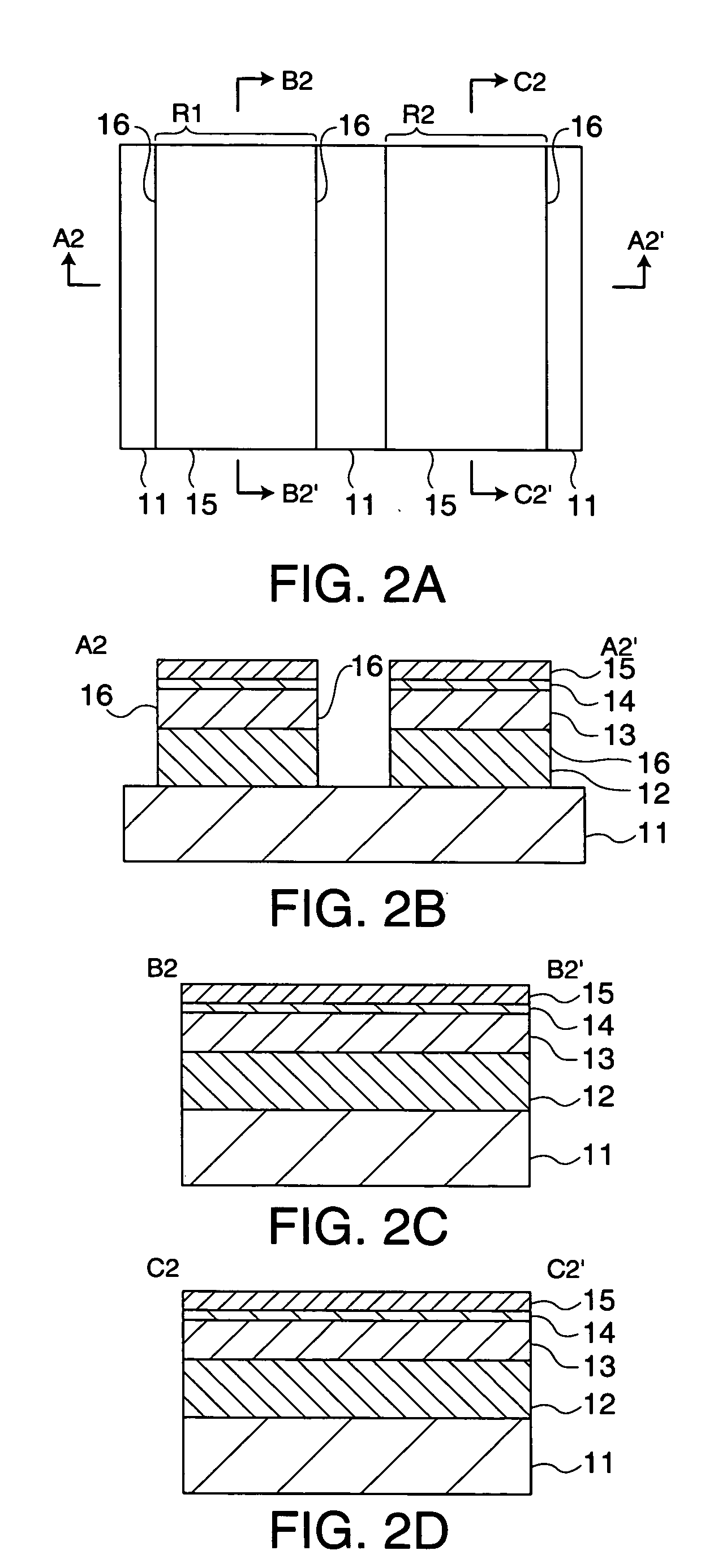
[0102]FIGS. 1A to 8A are top views each showing a method of manufacturing a semiconductor device according to a first embodiment of the invention, FIGS. 1B to 8B are cross sections along the lines A1-A1′ to A8-A8′ of FIGS. 1A to 8A, and FIGS. 1C to 8C are cross sections along the lines B1-B1′ to B8-B8′ of FIGS. 1A to 8A.

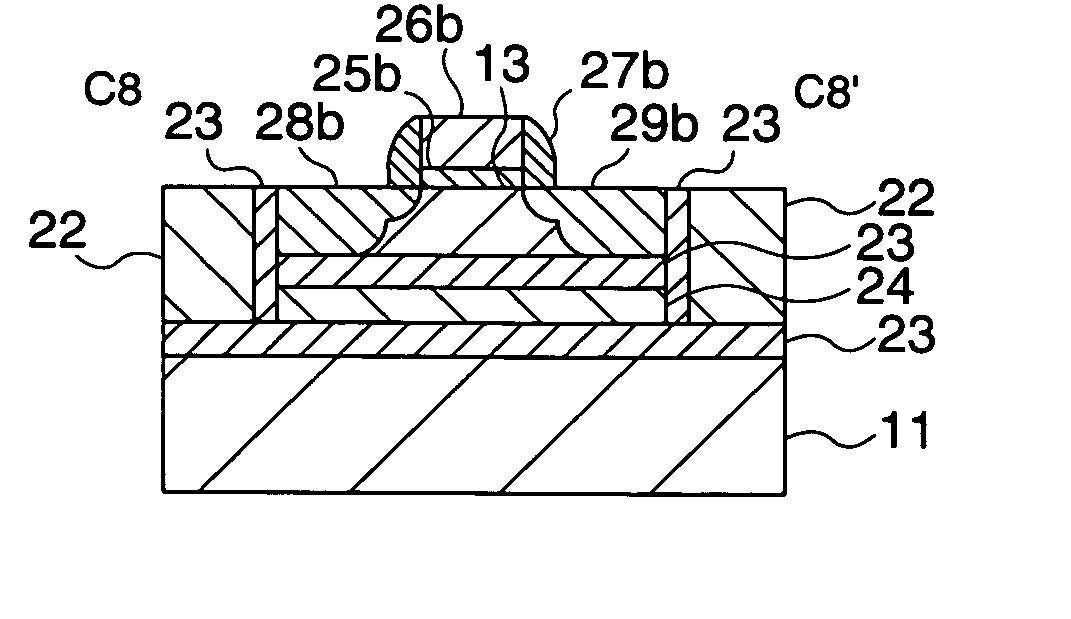
[0103] In FIGS. 1A to 1D, a first semiconductor layer 12 is formed on a semiconductor substrate 11 by epitaxial growth, and a second semiconductor layer 13 is formed on the first semiconductor layer 12 by epitaxial growth. As the first semiconductor layer 12A, it is possible to use a material that has a larger etching rate than the semiconductor substrate 11 and the second semiconductor layer 13. As materials of the semiconductor substrate 11, the first semiconductor layer 12, and the second semiconductor layer 13, it is possible to use a combination of what are selected from among Si, Ge, SiGe, SiC, SiSn, PbS, GaAs, InP, GaP, GaN, ZnSe, or the like. In particular, ...

second embodiment

[0123]FIGS. 9A to 16A are top views each showing a method of manufacturing a semiconductor device according to a second embodiment of the invention, FIGS. 9B to 9B are cross sections along the lines A21-A21′ to A28-A28′ of FIGS. 9A to 16A, and FIGS. 9C to 16C are cross sections along the lines B21-B21′ to B28-B28′ of FIGS. 9A to 16A.

[0124] In FIG. 9, semiconductor layer 151, 133, 152, and 135 are sequentially formed on a semiconductor substrate 131 by epitaxial growth. As the semiconductor layers 151 and 152, it is possible to use a material with a larger etching rate than the semiconductor substrate 131 and the semiconductor layers 133 and 135. In particular, when the semiconductor substrate 131 is Si, SiGe is preferably used as a material of the semiconductor layers 151 and 152, Si as a material of the semiconductor layers 133 and 135.

[0125] Thereafter, a base oxidation film 153 is formed on the surface of the semiconductor layer 135 by thermal oxidation, CVD, or the like of the...

third embodiment

[0136]FIGS. 17A to 26A are top views each showing a method of manufacturing a semiconductor device according to a third embodiment of the invention, FIGS. 17B to 17B are cross sections along the lines A31-A31′ to A40-A40′ of FIGS. 17A to 26A, and FIGS. 17C to 26C are cross sections along the lines B31-B31′ to B40-B40′ of FIGS. 17A to 26A.

[0137] In FIG. 17, a first semiconductor layer 212 is formed on a semiconductor substrate 211 by epitaxial growth, and a second semiconductor layer 213 is formed on the first semiconductor layer 212 by epitaxial growth. As the first semiconductor layer 212, it is possible to use a material that has a larger etching rate than the semiconductor substrate 211 and the second semiconductor layer 213. As materials of the semiconductor substrate 211, the first semiconductor layer 212, and the second semiconductor layer 213, it is possible to use a combination of what are selected from among Si, Ge, SiGe, SiC, SiSn, PbS, GaAs, InP, GaP, GaN, ZnSe, and the ...


PUM


Abstract

A semiconductor device includes a semiconductor layer formed on a semiconductor substrate by epitaxial growth, a first embedded insulating layer embedded in a first region between the semiconductor substrate and the substrate layer, and a second embedded insulating layer embedded in a second region between the semiconductor substrate and the semiconductor layer, wherein the first embedded insulating layer and the second embedded insulating layer are mutually different in at least either of effective work function and fixed charge amount.

Description

BACKGROUND [0001] 1. Technical Field [0002] The present invention relates to a semiconductor device and a method of manufacturing the same, particularly to a semiconductor device that is preferably applied to a semiconductor device having an embedded insulating layer formed on the back of an silicon on insulator (SOI) transistor. [0003] 2. Related Art [0004] Much attention has been paid to the utility of a field effect transistor formed on an SOI substrate in view of its ease of element isolation, being latchup-free, small source / drain joint capacitance, and the like. [0005] In JP-A-1998-261799, for example, disclosed is a method of forming a silicon thin film having excellent crystallinity and uniformity on an insulating film with a large area, by irradiating an ultraviolet beam to an amorphous or polycrystalline silicon layer formed on an insulating film in a pulse-shape to form a polycrystalline silicon film, in which single crystal particles shaped in nearly a square are arrange...

Claims


Application Information

Patent Timeline
IPC IPC(8): H01L29/792
CPCH01L21/84H01L27/1203H01L29/66772H01L29/78603H01L29/78654H01L21/20
Inventor KATO, JURI
Owner SEIKO EPSON CORP
Why Eureka
Try Eureka