Structures and processes for controlling access to optical media

a technology of optical media and control structures, applied in the direction of protective material radiating elements, instruments, recording signal processing, etc., can solve the problem that the player is not able to effectively read the disc, and achieve the effect of facilitating state change, reducing transition edge effects, and reducing interferen

Inactive Publication Date: 2007-06-21
NXP BV
View PDF22 Cites 23 Cited by
  • Summary
  • Abstract
  • Description
  • Claims
  • Application Information

AI Technical Summary

Benefits of technology

[0007] Briefly, the present invention provides an optical disc with an associated optical shutter. The optical shutter has at least two states. In a first state, the optical media interferes with the ability of an interrogating laser beam to read data from the optical media, and in a second state, the optical media is substantially transparent, enabling the laser beam to read the disc. A powering circuit is used to cause the optical shutter to transition from a first state to the second state. In one example, an integrated circuit acts as the powering circuit, as well as providing logic and processing functions. The integrated circuit also couples to an RF antenna, enabling the integrated circuit to communicate with an associated RF scanning device. The optical shutter may take various geometric shapes, and typically has an electrochromic material for facilitating state change. The electrochromic material may fill the shutter, or the material may form a pattern. The shutter may be positioned on the disk so that transition edge-effects are reduced, allowing for reduced interference with the laser beam when the optical shutter is in its clear state. The optical shutter does not cover the entire data area of the disc, and in one example,

Problems solved by technology

Since this area contains important information regarding the overall co

Method used


Image

  • Structures and processes for controlling access to optical media
  • Structures and processes for controlling access to optical media
  • Structures and processes for controlling access to optical media

Examples


example 1

EC device with MoO3+AlF3 Counterelectrode Processed by PVD

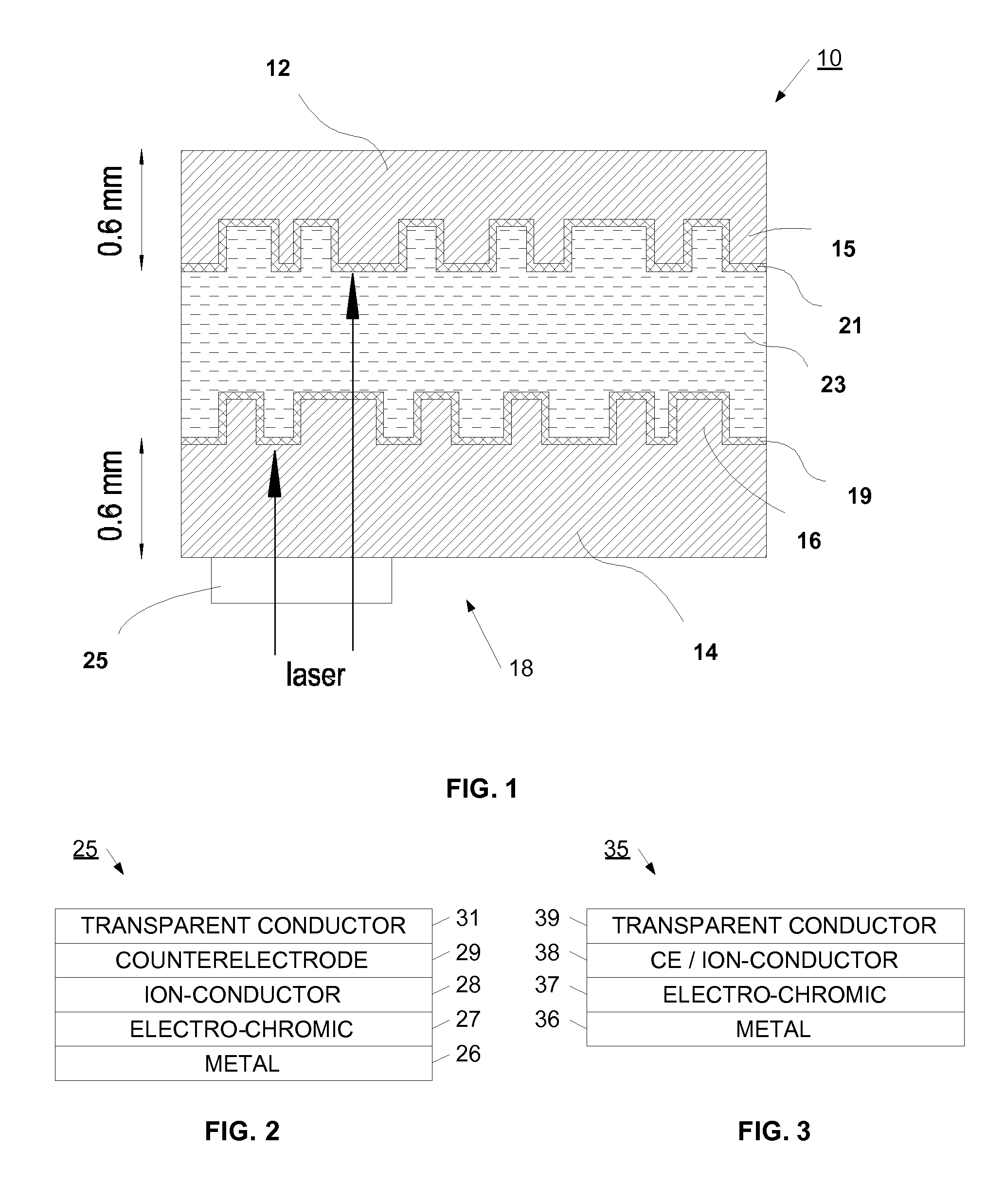
[0088] A set of four EC devices were fabricated on a conductive tin oxide coated glass by depositing coatings using physical vapor deposition (PVD). This was a five layer device similar to the one shown in FIG. 2 comprising of an EC layer, ion conductor and a counterelectrode sandwiched between two conductors. The devices were appropriately masked from each other to generate four independent devices in a size of about 1.5 cm×1.5 cm. The first layer was 500 nm tungsten oxide evaporated by an electron beam. Then 60 nm thick lithium metal was evaporated to dope and reduce tungsten oxide to its colored bronze (corresponding to about 24 mC / sq.cm of charge). An ion conductor comprising aluminum fluoride and lithium was deposited next in a thickness of 500 nm. This was followed by a counter electrode comprising about equal proportions of molybdenum oxide and aluminum fluoride in a thickness of 100 nm and the top conductor which was...

example 2

EC Device with NiO Counterelectrode Processed by PVD

[0089] Another set of devices was fabricated as in Example 1. however, in this case the counterelectrode was 120 nm thick nickel oxide. At 650 nm, this device in colored state was 2.6% transmitting and in the bleached state the transmission was 15.1%. The colored state transmission at 405 nm was 6.9% and 22.6% when bleached.

example 3

Electrochromic Polyaniline (PA) Coating

[0090] PA was deposited on ITO coated glass. The coating was deposited from a solution comprising formic acid and ascorbic acid. The coated substrate was heated to 70° C. for 15 minutes to remove the volatile products and solidify the coating. The 300 nm thick coatings were colorless as produced and were electrochromic as shown in FIG. 12 and the table below. FIG. 12 has a graph 120 that shows a % Transmission 121 versus wavelength 122 for the ITO substrate 123, the reduced PA 124, and the oxidized PA 125.

% Transmission at650 nm550 nm405 nmPolyanilineBleached71.675.852.8Colored28.750.018.2ITO substrate only84.087.773.4


PUM


Abstract

An optical disc is provided with an associated optical shutter. In a first state, the optical media interferes with the ability of an interrogating laser beam to read data from the optical media, and in a second state, the optical media is substantially transparent, enabling the laser beam to read the disc. A powering circuit is used to cause the optical shutter to transition from a first state to the second state. In one example, an integrated circuit acts as the powering circuit, as well as providing logic and processing functions. The integrated circuit also couples to an RF antenna, enabling the integrated circuit to communicate with an associated RF scanning device. The optical shutter may take various geometric shapes, and typically has an electrochromic material for facilitating state change. The electrochromic material may fill the shutter, or the material may form a pattern. The shutter may be positioned on the disk so that transition edge-effects are reduced, allowing for reduced interference with the laser beam when the optical shutter is in its clear state. The optical shutter does not cover the entire data area of the disc, and in one example, the optical shutter is quite small, allowing for lower cost production, as well as reducing power requirements to transition the electrochromic material. Power requirements may be further reduced by forming the electrochromic in a pattern. A small optical shutter may disable reading of disc, for example, by placing the small shutter over an important section of the disc, such as the lead-in area.

Description

RELATED APPLICATIONS [0001] This application claims priority to U.S. patent application No. 60 / 703,673, filed Jul. 29, 2005, and entitled “Devices for Optical Media”, and to U.S. patent application No. 60 / 720,986, filed Sep. 27, 2005, and entitled “Devices and Processes for Optical Media”, both of which are incorporated by reference as if set forth in their entirety. This application is also related to U.S. patent application No. ______, filed ______, and entitled, “Stable Electrochromic Device”, which is also incorporated by reference.FIELD OF THE INVENTION [0002] The present invention relates to an integrated circuit device and electro-optical materials that cooperate to enable selective access to content stored on an optical media. In one example, the present invention provides a method and system for use of an optical device to reduce theft of optical media, deny or enable access to content stored within or on optical media, and for communicating an aspect of optical media via p...

Claims


Application Information

Patent Timeline
IPC IPC(8): G11B23/03G02F1/1524
CPCG02F1/15G02F1/1508G02F1/1523G11B7/24033G11B7/24038G11B7/252G11B20/00086G11B20/00608G11B20/00666G11B20/00876G11B20/00927G11B23/0028G11B23/0035G11B23/0042G11B23/282G11B23/286G11B2220/2537H01Q1/2208H01Q1/40H01Q1/44G02F1/15165G02F1/1524
Inventor AGRAWAL, ANOOPRILUM, JOHN H.CRONIN, JOHN P.TONAZZI LOPEZ, JUAN CARLOSATKINSON, PAULMARQUARDT, RICKPARSONS, STEVE
Owner NXP BV
Why Eureka
Try Eureka