

Low loss silicon oxynitride optical waveguide, a method of its manufacture and an optical device
- Summary
- Abstract
- Description
- Claims
- Application Information
AI Technical Summary
Benefits of technology
Problems solved by technology
Method used
Image

Examples
example 1
[0159] A PECVD core glass has been grown on a standard PECVD apparatus (in this case a standard cluster tool CVD process chamber type PECVD-apparatus from STS (Surface Technology Systems plc of Newport, South Wales, UK) is used for the formation of layers on a silicon substrate using the following parameters:
[0160] a) SiH4 flow rate: 20 sccm
[0161] b) N2O flow rate: 100-400 sccm
[0162] c) N2 flow rate: 2000 sccm
[0163] d) 5% PH3 in N2 flow rate: 10 sccm
[0164] e) Power: 700 W
[0165] f) Pressure: 250 mTorr
[0166] g) Temperature: 350° C.
[0167] h) Frequency: 380 kHz
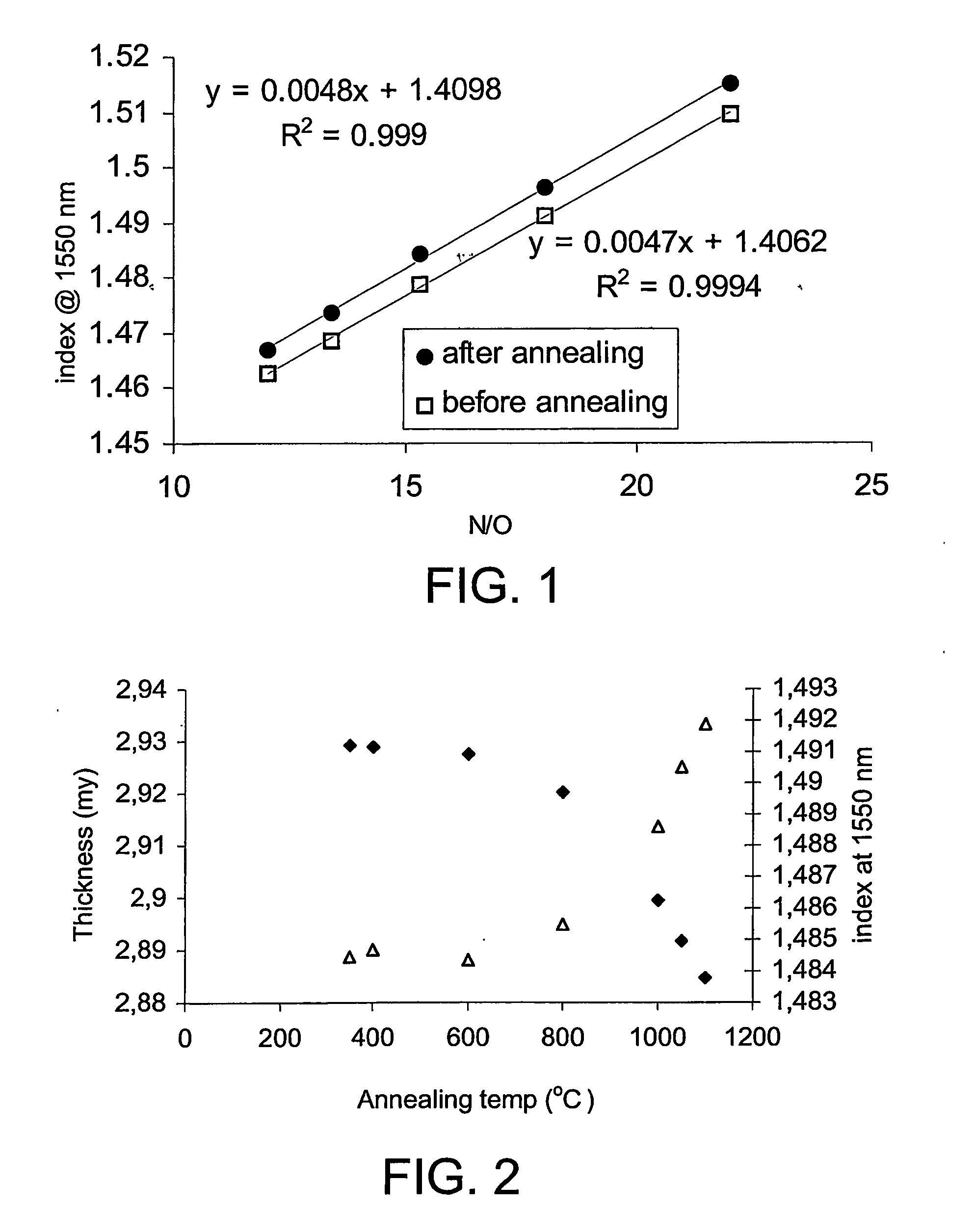
[0168]FIG. 1 shows the refractive index at λ=1550 nm for the core region of various optical waveguides according to the invention, before and after annealing, respectively. Annealing was performed at 1100° C. for 4 hours in a nitrogen atmosphere.
[0169] The refractive index may easily be tuned in a fairly large range and significantly larger than indicated in FIG. 1. The refractive index change is completely governed by t...
example2
[0190] A sample comprising an optical waveguide according to the invention was made as described in example 1 with the only difference that the 5% PH3 / 95% N2 gas flow was increased from 10 to 50 sccm. The hereby grown PECVD films delaminated upon annealing due to the high P-content. Thus, there is an upper limited to the amount of PH3 which can be present under PECVD growth of a core under the above mentioned process parameters.
example 3
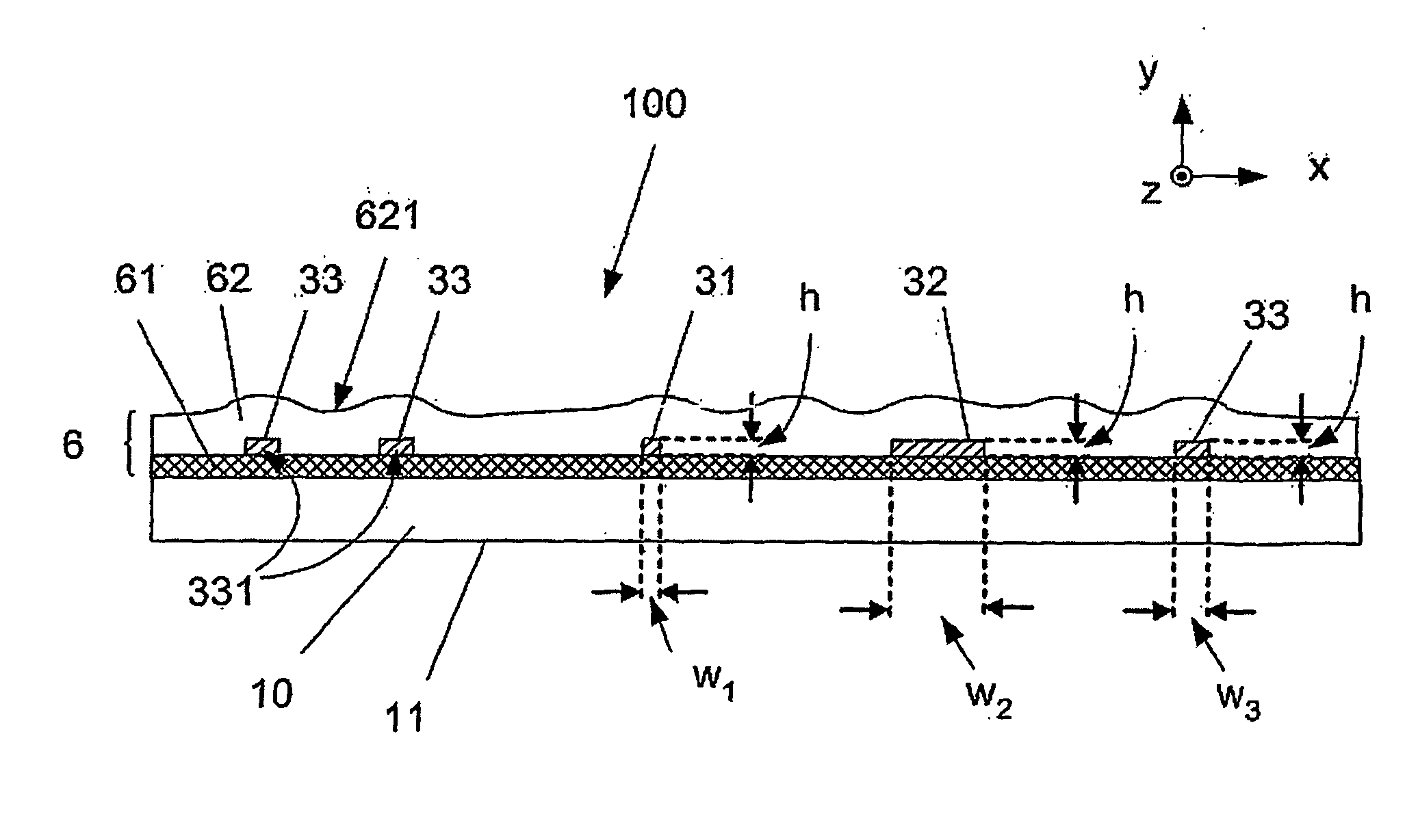
[0191] A sample comprising an optical waveguide according to the invention was made as described in example 1. The structure of the resulting waveguides were subsequently analyzed by Scanning Electron Microscopy (SEM) of polished cross sectional cuts. FIG. 7a shows the resulting waveguide profiles for an isolated waveguide 100 comprising core 33, lower 61 and upper 62 cladding regions. From FIG. 7a, it is evident that the waveguide core 33 (having a width of app. 7 μm as indicated in the SEM-photo) is (partially) surrounded by the upper cladding layer 62, and furthermore, no defects can be seen close to the waveguide core region. For closer spaced waveguides (e.g. for edge-to-edge spacings 72 less than 4 μm, cf. FIG. 7b), one observes an apparent reaction between the (upper) cladding layer 62 and the waveguide core material 33 resulting in the nucleation and growth of small crystallites / particles 71 next to the waveguide core regions. FIG. 7b shows a representative SEM image of this...
PUM
| Property | Measurement | Unit |
|---|---|---|
| Temperature | aaaaa | aaaaa |
| Temperature | aaaaa | aaaaa |
| Temperature | aaaaa | aaaaa |
Abstract
Description
Claims
Application Information