

Method for fabricating an integrated circuit on a semiconductor substrate
- Summary
- Abstract
- Description
- Claims
- Application Information
AI Technical Summary
Benefits of technology
Problems solved by technology
Method used
Image

Examples
first embodiment
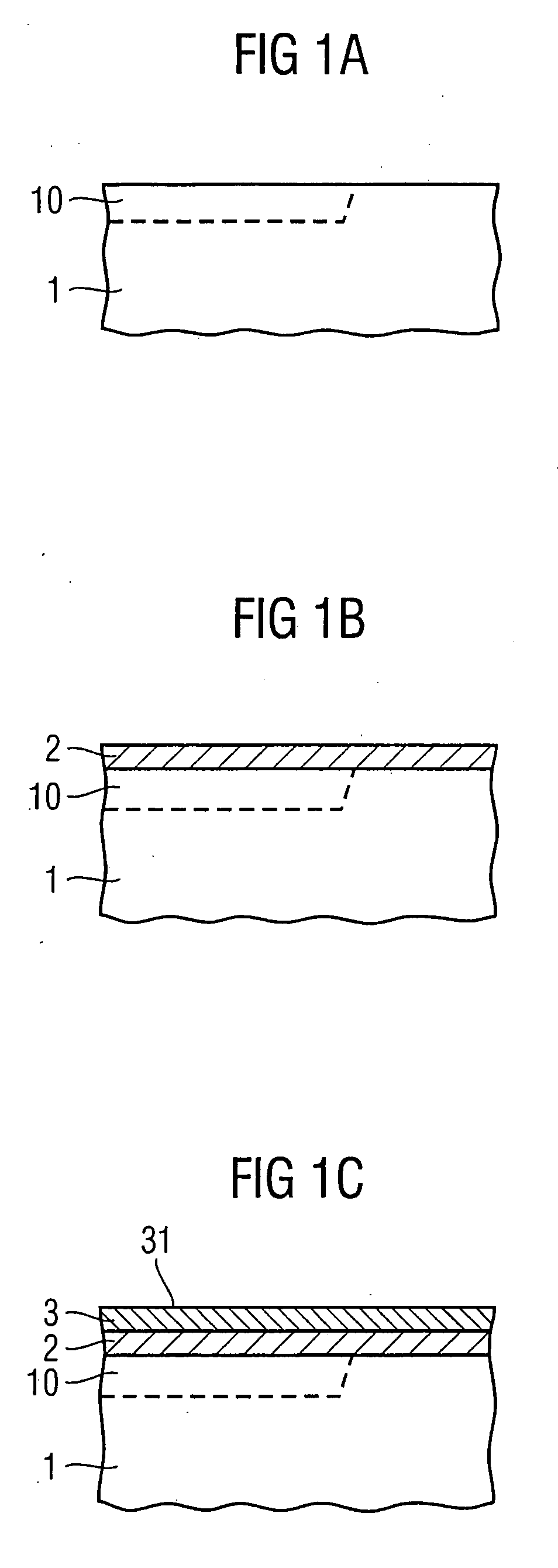
[0032]FIG. 1 shows a section of an integrated device as a schematic view, according to the present invention. As shown in panel A, the integrated device is formed on a semiconductor substrate 1. This semiconductor substrate 1 may comprise functional elements or layers 10, for example conductive or dielectric layers, or doped regions within the substrate 1.
[0033] As shown in panel B, a conductive layer 2 is deposited on the functional elements or layers 10 on the substrate 1. Said conductive layer 2 may cover only parts of the functional elements or layers 10 and may also extend to other parts of the substrate 1.
[0034] In a subsequent process stage, as shown in panel C, a counter-stress layer 3 is deposited on the conductive layer 2. Said counter-stress layer 3 preferably provides an amorphous or crystalline surface 31. In this way, the surface 31 lacks distinct features, such as grain boundaries or other features that may act as crystallization seeds or may influence a phase change...
third embodiment
[0044]FIG. 3 shows a detailed view of sections of the integrated device shown in FIG. 2, according to a second and third embodiment of the present invention.
second embodiment
[0045] Panel 3A shows a detailed view of the layer setup at the interface of a dielectric element 214 and a poly-silicon element 214 located in the region 210 of FIG. 2. According to this second embodiment, a conductive layer 302 is adjacent to a dielectric element 301. Between the conductive layer 302 and a poly-silicon element 304, an intermediate counter-stress layer 303 is arranged. Said intermediate counter-stress layer 303 allows for a stress-reduced crystallization of the poly-silicon layer 304 from an initially amorphous state. The intermediate counter-stress layer 303 may be low-resistive or may comprise pores 305, such to enable direct electric contact between the poly-silicon element 304 and the conductive layer 302.
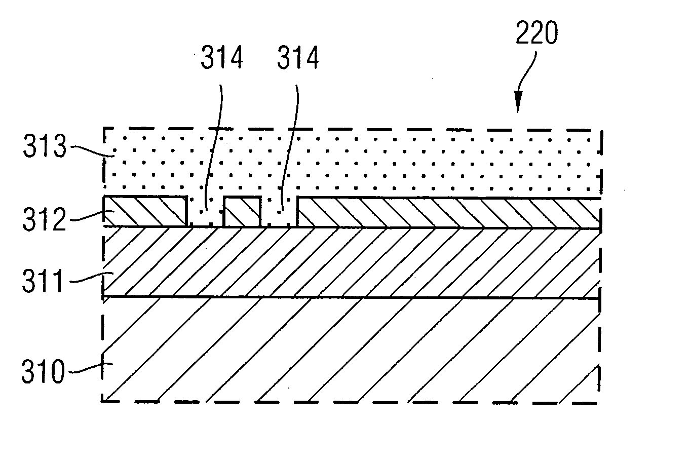
[0046] Panel B shows the section 220 of FIG. 2, according to a third embodiment of the present invention. In this section 220, a gate dielectric element 310 is covered by a conductive layer 311. A poly-silicon element 313 is arranged on top of the conductive l...
PUM
 Abstract
Description
Claims
Application Information