Low-noise image sensor and transistor for image sensor

a low-noise, image sensor technology, applied in the direction of electrical equipment, semiconductor devices, radio frequency control devices, etc., can solve the problems of image lag, incomplete charge transfer, image lag, etc., to improve the well capacity, enhance the performance of the image sensor, and raise the barrier

Inactive Publication Date: 2007-07-12
ELECTRONICS & TELECOMM RES INST
View PDF20 Cites 11 Cited by
  • Summary
  • Abstract
  • Description
  • Claims
  • Application Information

AI Technical Summary

Benefits of technology

[0031] In the present invention, three improvements are presented to enhance a performance of an image sensor due to dark current reduction and so forth.
[0032] First, in a light integration region, a region of a photodiode to which light is applied, a negative offset potential is applied to a transfer transistor or another transistor corresponding to the transfer transistor, thereby raising a barrier and improving well capacity, and a trap disposed around the transistor is deactivated by holes accumulated around the transistor, and thus the dark current is reduced. Since the hole accumulation is achieved by negative offset bias rather than p type doping, transfer transistor should have low threshold voltage. As a result, complete photodiode reset may be performed by a structure capable of using a high overdrive voltage (that is, the transfer transistor transfers enough charges). Also, when the photodiode is reset, the photodiode is depleted at a low voltage and then the barrier is raised by an external terminal so as to reset the transistor, and thus the efficiency of the well capacity may increase when the transistor is reset.
[0033] Second, a sub gate oxide for forming the transfer transistor is included to maximize the application of the negative offset potential according to the first aspect, and is disposed to overlap a part of a light receiving part of the photodiode.
[0034] Third, the dark current caused by a trench region is reduced by limiting reception of light around the trench region of the light receiving part of the photodiode.

Problems solved by technology

However, in general, increased capacity of the photodiode results in image lag caused by the incomplete transfer of charges.
However, this may cause the incomplete transfer of charges.
324-327), a pinning voltage higher than a gate turn-on voltage makes an operation of a transistor into a sub threshold region, and this results in image lag caused by incomplete reset and transfer process.
This results in degradation of image quality.
However, even if the junction profile is optimized, incomplete reset or incomplete charge depletion in an N well of a pinned photodiode occurs in some conditions, and thereby image lag is caused.
Particularly, as a power supply voltage is more lowered for a low power operation, such a CMOS process and scaling of a device make these problems worse.
The severest problem is incomplete charge depletion in the N well of the photodiode at a low operating voltage, for example, at 2.5V or less.
For this reason, the image lag occurs, which results in deterioration of SNR at low illumination.
Thus, such incomplete reset may be overcome by providing a lower threshold voltage of the transfer transistor, but thereby a well capacity of the PDD is reduced, and sufficient impedance may not be generated when the transfer transistor is turned off, which results in more decrease in the well capacity.
In other words, if the threshold voltage of the transfer transistor is lowered in order to thoroughly and rapidly reset or transfer electrons, a sufficient barrier may not be formed when the transfer transistor is turned off, so that the well capacity decreases.
On the other hand, if the threshold voltage of the transfer transistor is increased, a sufficient barrier is formed so that the well capacity may largely increase, but in this case, electrons are reset in the sub threshold region and then transferred, which results in incomplete depletion.
However, this method cannot be continuously used at a low power supply voltage.
This is because the photodiode is lightly doped, making it difficult to further lower a pinning voltage, and a voltage itself applied to the transfer transistor is already too low.
However, in the suggested structure, well capacity is not improved, and dark current may increase depending on actual realizations.
The severest problem caused by lowering an operating voltage is that a turn-on voltage of the transfer transistor is not higher enough than a threshold voltage of the transfer transistor, so that a photodiode moves to a sub threshold region before it is fully depleted.
As a result, the conventional arts described above cannot be appropriate solutions for overcoming the above problems because they may not improve well capacity and depletion efficiency at the same time.
Still another cause of dark current is shallow trench isolation (STI).
However, the ion implantation into the region under the trench results in high leakage of current, which functions as dark current.
In particular, when ions are injected into a substrate adjacent to edges of the trench, current leakage may occur in junctions between active device regions and the trenches.

Method used


Image

  • Low-noise image sensor and transistor for image sensor
  • Low-noise image sensor and transistor for image sensor
  • Low-noise image sensor and transistor for image sensor

Examples


exemplary embodiment 1

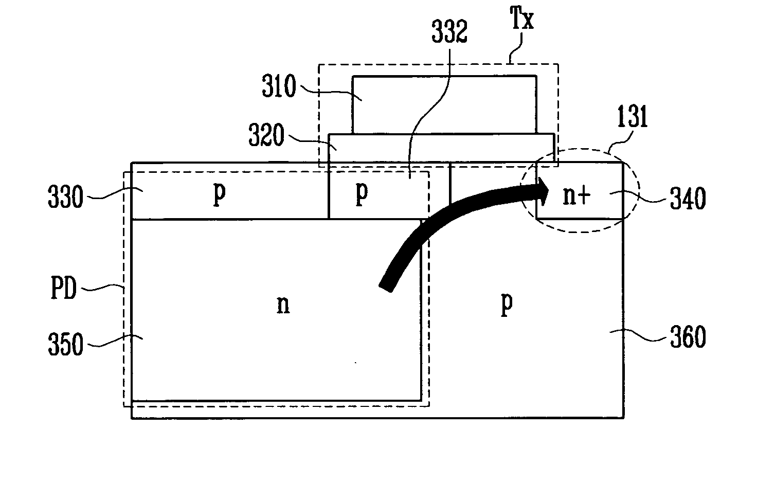
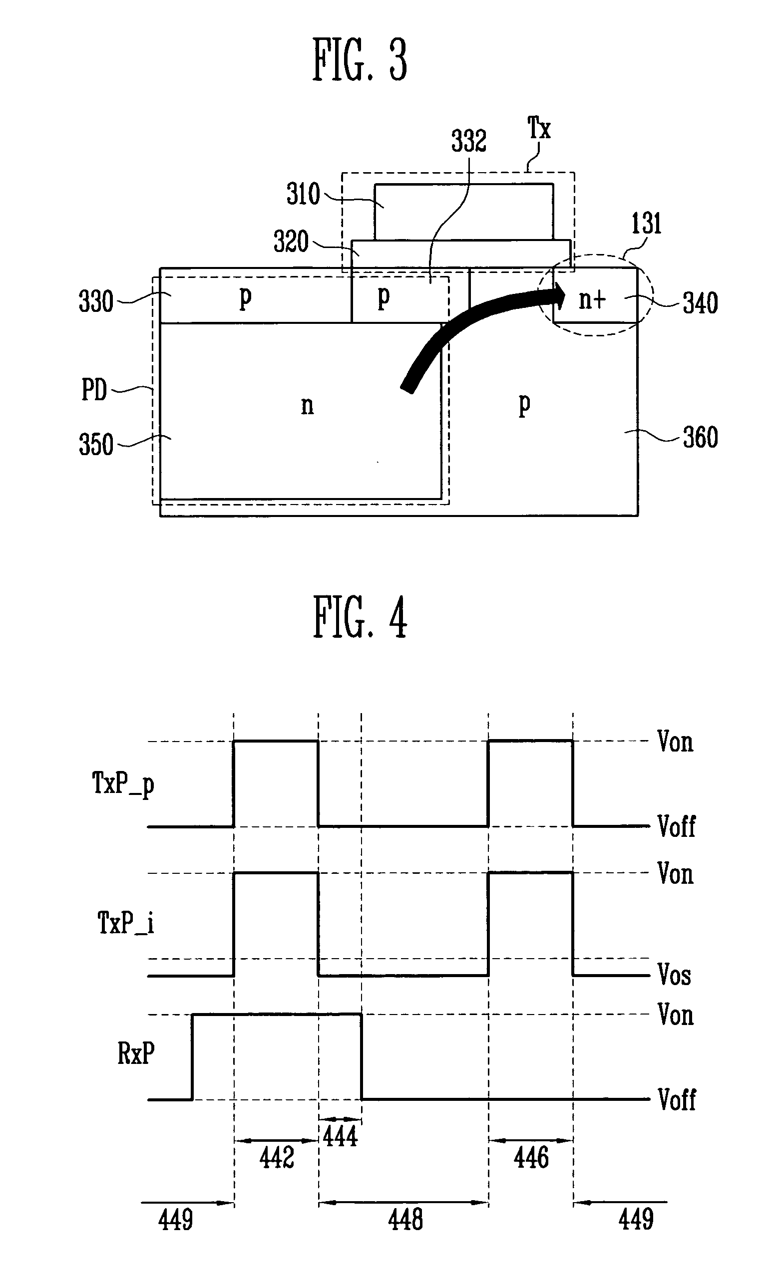
[0044]FIG. 3 is a cross-sectional view of a 4-transistor pixel structure according to an exemplary embodiment of the present invention. Though the exemplary embodiment specifically describes the aspect of the present invention is applied to a transfer transistor, this is only an example for convenience of descriptions because a transfer transistor has the highest efficiency. Thus, it is apparent that the aspect of the invention may also be applied to other transistor devices in an image sensor (particularly, a reset transistor with a function of transferring charges), which is also in the scope of the present invention.

[0045]FIG. 3 only illustrates a photodiode PD, a transfer transistor Tx and a floating diffusion region 131 in the 4-transistor pixel structure. The transfer transistor Tx comprises a gate 310, a gate oxide layer 320 and a p-type substrate 360, the photodiode PD region comprises a photodiode (n-type) doped region 350 and a surface p-doped region 330, and the diffusio...

exemplary embodiment 2

[0056] The exemplary embodiment relates to a transfer transistor having an optimized stack structure for the control method for the transfer transistor illustrated in FIG. 4. Though the exemplary embodiment specifically describes the aspect of the present invention is applied to a transfer transistor, this is only an example for convenience of descriptions because a transfer transistor has the highest efficiency. Thus, it is apparent that the aspect of the invention may also be applied to other transistor devices in an image sensor (particularly, a reset transistor with a function of charge transfer), which is also in the scope of the present invention.

[0057] A transfer transistor illustrated in FIG. 5 includes a main gate oxide 520 disposed on a charge transfer channel from a photodiode to a diffusion node; a main gate electrode 510 disposed on the main gate oxide 520; a sub gate oxide 522 extending from the main gate oxide 520 and overlapping a part of the photodiode; and a sub g...

exemplary embodiment 3

[0062] The present exemplary embodiment relates to an image sensor having an optimal structure for suppressing dark current according to a third aspect of the present invention. Here, the image sensor may be modified entirely or partially.

[0063] The image sensor illustrated in FIG. 6 includes: a diffusion node region 620; a photodiode region 610; a transfer transistor for forming a charge transfer channel between the diffusion node and the photodiode; and a dark current removal electrode 640 electrically connected with a gate electrode 630 of the transfer transistor, and insulated from a part of the photodiode region in which dark current is generated and overlapping the part.

[0064] The dark current removal electrode 640 may be a transparent electrode, for example, formed of ITO, to increase photon absorbing efficiency in the photodiode region 610 under the dark current removal electrode 640, and form an oxide layer under the photodiode region 610 to ensure an electrically insulat...


PUM


Abstract

Provided are a low-noise image sensor capable of improving the efficiency of charge transfer from a photodiode to a diffusion node region and effectively suppressing the generation of dark current, and a transistor for the image sensor. The image sensor includes: a photosensitive pixel having a transfer transistor formed in a structure which causes hole accumulation in a part or all regions of a gate oxide; and a sensing control part applying a negative offset potential to the gate during a part or whole of a turn-off period of the transfer transistor. When the transfer transistor is off, the image sensor may form a sufficient barrier and accumulate electrons in the photodiode, and when the transistor is on, the sensor sufficiently lowers a barrier, fully depletes the photodiode before the transfer transistor reaches a threshold voltage, and inactivates a trap in a predetermined region for a certain time, and thus the dark current can be reduced.

Description

CROSS-REFERENCE TO RELATED APPLICATION [0001] This application claims priority to and the benefit of Korean Patent Application Nos. 2005-117419, filed Dec. 5, 2005, and 2006-87439, filed Sept. 11, 2006, the disclosures of which are incorporated herein by reference in their entirety. BACKGROUND [0002] 1. Field of the Invention [0003] The present invention relates to a low-noise image sensor and a transistor for the image sensor, and more particularly, to a low-noise image sensor capable of improving the efficiency of charge transfer from a photodiode to a diffusion node region and effectively suppressing the generation of dark current and enhancing well capacity, and a transistor for the image sensor. [0004] 2. Discussion of Related Art [0005] Image sensors may be classified into a charge-coupled device (CCD) sensor and a CMOS image sensor, which basically utilize an electron-hole pair separated by light having a higher energy than a silicon bandgap. In image sensors, an amount of ir...

Claims


Application Information

Patent Timeline
Patent Type & Authority Applications(United States)
IPC IPC(8): H01L31/113H01L31/062
CPCH01L27/14603H01L27/14601H01L27/14614H01L27/146
Inventor MHEEN, BONG KIKIM, MI JINSONG, YOUNG JOO
Owner ELECTRONICS & TELECOMM RES INST
Why Eureka
Try Eureka