High-throughput printing of chalcogen layer and the use of an inter-metallic material

a chalcogen layer and high-throughput technology, applied in the field of solar cells, can solve the problems of poor surface coverage, difficult and difficult to use traditional vacuum-based deposition process to achieve precise stoichiometric composition over relatively large substrate area

a chalcogen layer and high-throughput technology, applied in the field of solar cells, can solve the problems of poor surface coverage, difficult and difficult to use traditional vacuum-based deposition process to achieve precise stoichiometric composition over relatively large substrate area

US20070163643A1Inactive Publication Date: 2007-07-19NANOSOLAR

Image

  • High-throughput printing of chalcogen layer and the use of an inter-metallic material
  • High-throughput printing of chalcogen layer and the use of an inter-metallic material
  • High-throughput printing of chalcogen layer and the use of an inter-metallic material

Examples


first embodiment

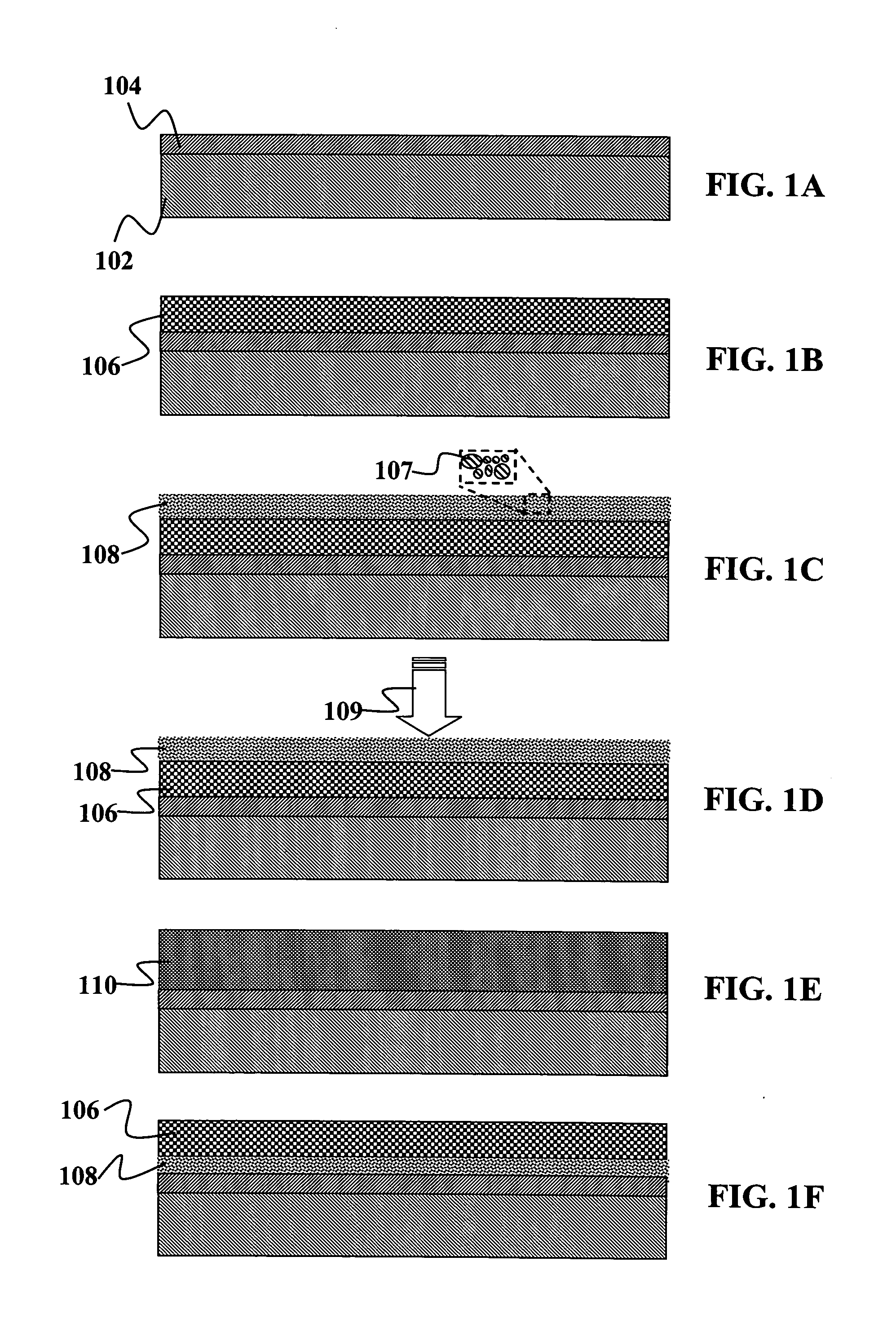
[0046] According to the present invention, the compound layer may include one or more group IB elements and two or more different group IIIA elements as shown in FIGS. 1A-1E.

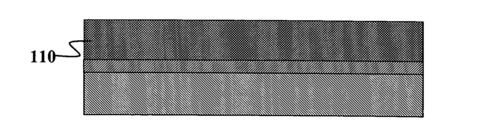
[0047] The absorber layer may be formed on a substrate 102, as shown in FIG. 1A. By way of the example, the substrate 102 may be made of a metal such as, but not limited to, aluminum. Depending on the material of the substrate 102, it may be useful to coat a surface of the substrate with a contact layer 104 to promote electrical contact between the substrate 102 and the absorber layer that is to be formed on it. For example, where the substrate 102 is made of aluminum the contact layer 104 may be a layer of molybdenum. For the purposes of the present discussion, the contact layer 104 may be regarded as being part of the substrate. As such, any discussion of forming or disposing a material or layer of material on the substrate 102 includes disposing or forming such material or layer on the contact layer 104, if o...

second embodiment

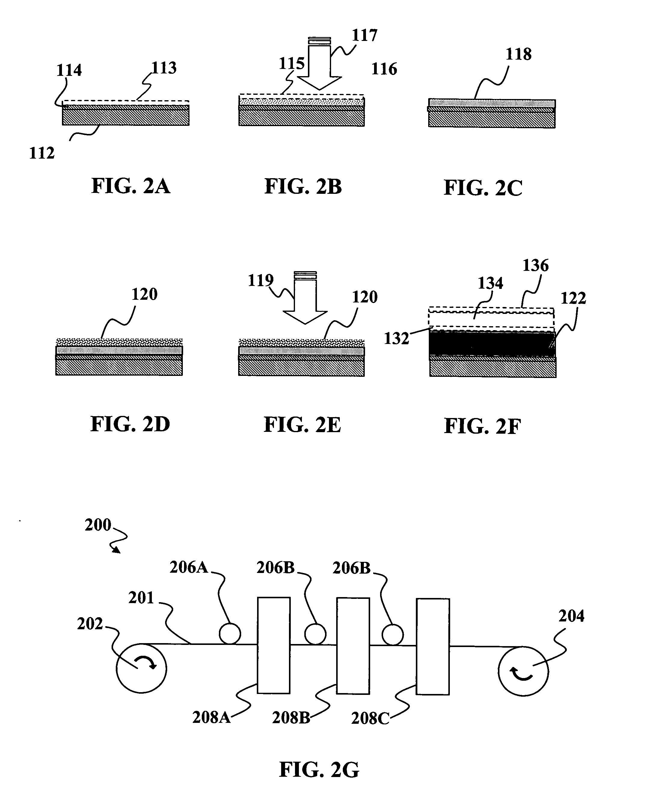
[0072] According to the present invention, the compound layer may include one or more group IB elements and one or more group IIIA elements. Fabrication may proceed as illustrated in FIGS. 2A-2F. The absorber layer may be formed on a substrate 112, as shown in FIG. 2A. A surface of the substrate 112, may be coated with a contact layer 114 to promote electrical contact between the substrate 112 and the absorber layer that is to be formed on it. By way of example, an aluminum substrate 112 may be coated with a contact layer 114 of molybdenum. As discussed above, forming or disposing a material or layer of material on the substrate 112 includes disposing or forming such material or layer on the contact layer 114, if one is used. Optionally, it should also be understood that a layer 115 may also be formed on top of contact layer 114 and / or directly on substrate 112. This layer may be solution coated, evaporated, and / or deposited using vacuum based techniques. Although not limited to the...


PUM

PropertyMeasurementUnit
Temperatureaaaaaaaaaa

Abstract

Methods and devices for high-throughput printing of a precursor material for forming a film of a group IB-IIIA-chalcogenide compound are disclosed. In one embodiment, the method comprises forming a precursor layer on a substrate, wherein the precursor layer comprises one or more discrete layers. The layers may include at least a first layer containing one or more group IB elements and two or more different group IIIA elements and at least a second layer containing elemental chalcogen particles. The precursor layer may be heated to a temperature sufficient to melt the chalcogen particles and to react the chalcogen particles with the one or more group IB elements and group IIIA elements in the precursor layer to form a film of a group IB-IIIA-chalcogenide compound. At least one set of the particles in the precursor layer are inter-metallic particles containing at least one group IB-IIIA inter-metallic alloy phase. The method may also include making a film of group IB-IIIA-chalcogenide compound that includes mixing the nanoparticles and / or nanoglobules and / or nanodroplets to form an ink, depositing the ink on a substrate, heating to melt the extra chalcogen and to react the chalcogen with the group IB and group IIIA elements and / or chalcogenides to form a dense film.

Description

CROSS-REFERENCE TO RELATED APPLICATION [0001] This application is a continuation-in-part of commonly-assigned, co-pending application Ser. No. 11 / 243,522 entitled “HIGH-THROUGHPUT PRINTING OF CHALCOGEN LAYER” filed Feb. 23, 2006, which is a continuation-in-part of commonly-assigned, co-pending application Ser. No. 11 / 290,633 entitled “CHALCOGENIDE SOLAR CELLS” filed Nov. 29, 2005 and Ser. No. 10 / 782,017, entitled “SOLUTION-BASED FABRICATION OF PHOTOVOLTAIC CELL” filed Feb. 19, 2004 and published as U.S. patent application publication 20050183767. This application is also a continuation-in-part of commonly-assigned, co-pending U.S. patent application Ser. No. 10 / 943,657, entitled “COATED NANOPARTICLES AND QUANTUM DOTS FOR SOLUTION-BASED FABRICATION OF PHOTOVOLTAIC CELLS” filed Sep. 18, 2004. This application is a also continuation-in-part of commonly-assigned, co-pending U.S. patent application Ser. No. 11 / 081,163, entitled “METALLIC DISPERSION”, filed Mar. 16, 2005. This application...

Claims


Application Information

Patent Timeline
19 Jul 2007
Publication
US20070163643A1
IPC
B05D3/00
CPC
C23C18/1204; H01L31/02008; H01L31/0322; Y02E10/541; H01L31/0749; H01L31/18; H01L31/048
Inventors
VAN DUREN, JEROEN K.J.; ROBINSON, MATTHEW R.