
Light emitting diode by use of metal diffusion bonding technology and method of producing light emitting diode

a light-emitting diode and metal diffusion bonding technology, applied in the direction of semiconductor/solid-state device manufacturing, electrical equipment, semiconductor devices, etc., can solve the problems of difficult to maintain the integrity of the bonded wafer or achieve a high yield rate, high operating voltage of the led, etc., and achieve the effect of improving performan

Inactive Publication Date: 2007-08-23
ARIMA OPTOELECTRONICS
View PDF4 Cites 64 Cited by
  • Summary
  • Abstract
  • Description
  • Claims
  • Application Information

AI Technical Summary

Benefits of technology

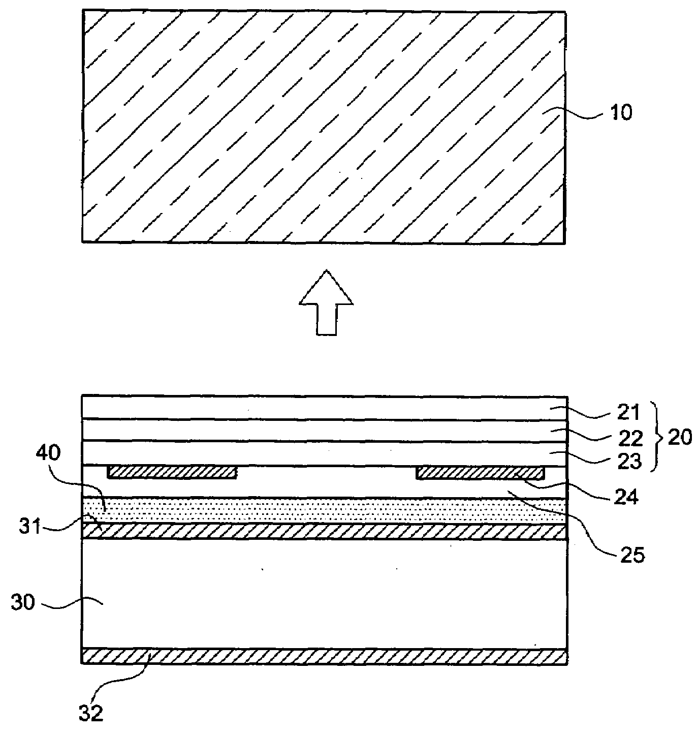
[0009]Therefore, the primary objective of present invention is to provide a manufacturing method of light emitting diode that utilizes metal diffusion bonding technology. AlInGaP light emitting diode epitaxial structure on a temporary substrate (GaAs) is bonded to a permanent substrate (such as GaP, GaAs, and Mo, etc) having a thermal expansion coefficient similar to that of the epitaxial structure, so as to produce an LED having a vertical structure and better performance.

Problems solved by technology

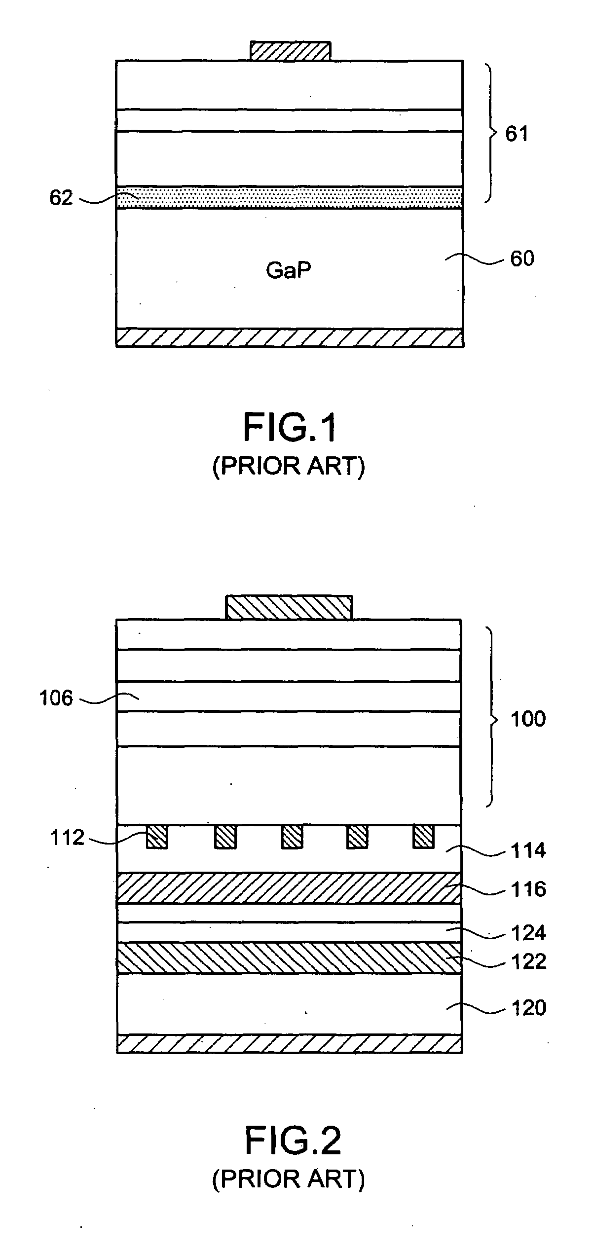
The fusion bonding process has the following drawbacks: (1) after the removal of the GaAs substrate, the remaining LED structure is very thin, e.g., ˜50 μm, and therefore fragile and difficult to handle, so that it is difficult to maintain the integrity of the bonded wafer or achieve a high yield rate; and (2) it is necessary to align precisely the lattice direction of LED structure and the permanent transparent substrate during the wafer bonding process, otherwise the operating voltage of the LED will be high.
This method has the following drawbacks: (1) Since this kind of eutectic reactions is fast, it is not easy to control the thickness of the metal bonding layer after bonding; (2) It is likely to produce an intermetallic compound (IMC) which is a fragile material, and the IMC further deteriorates the bonding strength; and (3) The bonded wafer can not go through a temperature higher than the bonding temperature in the chip process steps following wafer bonding, otherwise, the metal bonding layer will be affected.
Furthermore, the bonding strength is not strong enough to survive the long-term reliability test, which is essential for high brightness LED.
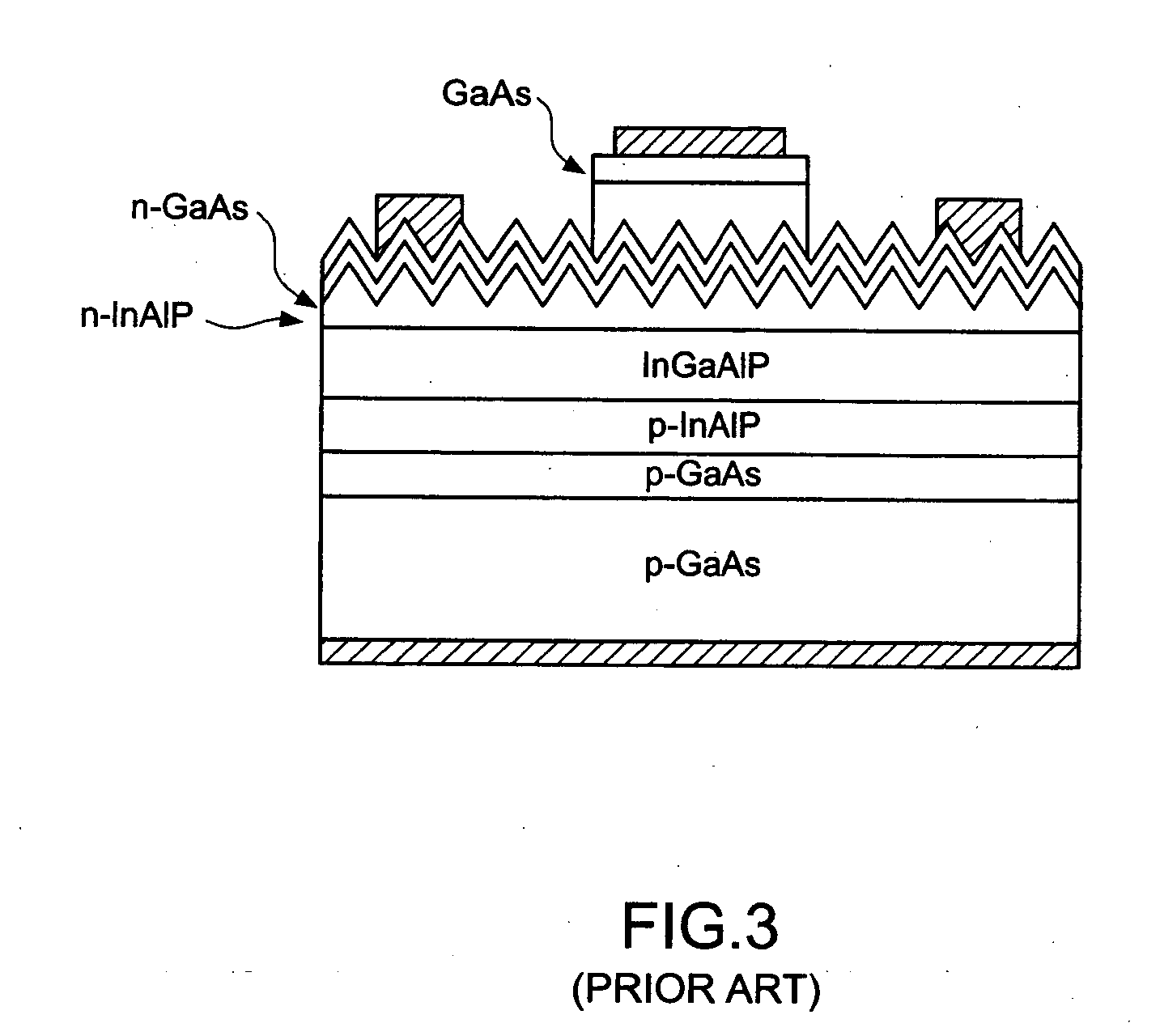
However, both methods cannot guarantee the uniformity of the surface roughness.
Such limitation makes the implementation of the surface roughening process of AlInGaP light emitting devices difficult.

Method used


Image

  • Light emitting diode by use of metal diffusion bonding technology and method of producing light emitting diode
  • Light emitting diode by use of metal diffusion bonding technology and method of producing light emitting diode
  • Light emitting diode by use of metal diffusion bonding technology and method of producing light emitting diode

Examples


Embodiment Construction

[0034]The AlInGaP semiconductor LED is, in general, grown on the GaAs substrate. GaAs substrate is a light-absorbing substrate that will absorb most of the light emitted from the active layer toward the substrate. The present invention employs a wafer bonding method to replace GaAs substrate with a permanent thermal and electrical conductive substrate. With the disclosed chip structures, light from the active layer will be reflected instead of absorbed by substrate. As a mechanical support to the epi layers, the bonding quality plays a very important role to the production yield. As a result, the chosen bonding process dramatically affects the cost of production. The aforementioned “Fusion Bonding” provides an excellent strength for the bonding interface due to its high bonding temperature and high bonding pressure. However, it is rather difficult to obtain a stable forward voltage with the above-mentioned technology. It is possibly a potential barrier at the bonding interface will ...


PUM


Abstract

The main objective of present invention is to provide a manufacturing method of light emitting diode that utilizes metal diffusion bonding technology. AlInGaP light emitting diode epitaxial structure on a temporary substrate is bonded to a permanent substrate having a thermal expansion coefficient similar to that of the epitaxial structure, and then the temporary substrate is removed to produce an LED having a vertical structure and better performance. The other objective of the present invention is to provide a high performance LED that uses metal diffusion technology and wet chemical etching technology to roughen the LED surface in order to improve light extraction efficiency.

Description

BACKGROUND OF THE INVENTION[0001]1. Field of the Invention[0002]The present invention relates generally to high-performance light emitting diodes, and more particularly to a method of using metal diffusion bonding technology as well as surface treatment process to improve light extraction efficiency.[0003]2. Description of the Related Art[0004]The MOCVD epitaxy technology has been applied in the production of high brightness Group III-V light emitting diodes (LEDs), which include aluminum indium gallium phosphide (AlInGaP, wavelength range: 560 nm˜650 nm) LEDs and indium gallium nitride (InGaN, wavelength range: 380 nm 550 nm) LEDs. High brightness LEDs are employed extensively in the areas of indicating lamps, traffic lights, outdoors displays, special lighting, etc. The epitaxial growth of AlInGaP LED is usually grown on lattice-matched GaAs substrate in order to get good crystal quality. However, since the energy bandgap of GaAs substrate is less than the emission energy of LED, ...

Claims


Application Information

Patent Timeline
IPC IPC(8): H01L33/00H01L33/06H01L33/22H01L33/30
CPCH01L33/0079H01L33/0093
Inventor SUNG, YING-CHEWANG, CHAO-HSINCHEN, YI-HSIUNGCHIU, SHIH-YU
Owner ARIMA OPTOELECTRONICS
Learn More