Strain enhanced CMOS architecture with amorphous carbon film and fabrication method of forming the same

a technology of amorphous carbon film and enhanced cmos, which is applied in the field of cmos devices, can solve the problems of high process cost, affecting device performance, and nmos and pmos devices requiring different types of stress

Inactive Publication Date: 2007-08-30
TAIWAN SEMICON MFG CO LTD
View PDF16 Cites 92 Cited by
  • Summary
  • Abstract
  • Description
  • Claims
  • Application Information

AI Technical Summary

Benefits of technology

[0003] Currently, the CMOS manufacturing techniques selectively address pMOS and nMOS devices. A pMOS fabrication method includes using substrate structures that apply a compression stress to the channel, and an nMOS fabrication method includes using a tensile film to improve carrier mobility. In one approach, using selective epitaxial SiGe in silicon recesses of the source and drain regions, longitudinal uniaxial compressive stress is introduced into the pMOS device to increase hole mobility. Also, using a tensile SiN capping layer on the gate structure, tensile strain is introduced into the nMOS device to enhance electron mobility. In the embedded SiGe source / drain approach, the SiGe profile in the silicon recess is critical for strain profile which impacts device performance greatly. However, the embedded SiGe process needs extra lithography, etching, hard mask film deposition and clean process, causing high process costs. Also, it is difficult to control the etching depth and the silicon recess profile since the recess etching process is a time-mode control without using an etching stop layer, thereby consuming heavy cost on process monitor. In addition, the tensile SiN capping layer, also serving as a contact etching stop layer (CESL), will be consumed by about 200 Angstroms and have poor uniformity in subsequent contact hole etching step by the use of dry strip on photoresist and BARC with O2 / H2 and CF4 flow gas, high power, significant ion bombardment and over-etch time control. A subsequent step for removing the CESL, a plasma process with an over-etch time control further causes significant loss of silicide and / or oxides on the contact bottom and / or at shallow trench isolation (STI) edge. The weak spots on the thinner silicide or the junction at the STI edge cause defects of shorts and / or high junction leakage, imposing severe limitations in forming shallow junctions.

Problems solved by technology

One problem facing CMOS manufacturing is that nMOS and pMOS devices require different types of stress in order to achieve increased carrier mobility.
In the embedded SiGe source / drain approach, the SiGe profile in the silicon recess is critical for strain profile which impacts device performance greatly.
However, the embedded SiGe process needs extra lithography, etching, hard mask film deposition and clean process, causing high process costs.
Also, it is difficult to control the etching depth and the silicon recess profile since the recess etching process is a time-mode control without using an etching stop layer, thereby consuming heavy cost on process monitor.
In addition, the tensile SiN capping layer, also serving as a contact etching stop layer (CESL), will be consumed by about 200 Angstroms and have poor uniformity in subsequent contact hole etching step by the use of dry strip on photoresist and BARC with O2 / H2 and CF4 flow gas, high power, significant ion bombardment and over-etch time control.
A subsequent step for removing the CESL, a plasma process with an over-etch time control further causes significant loss of silicide and / or oxides on the contact bottom and / or at shallow trench isolation (STI) edge.
The weak spots on the thinner silicide or the junction at the STI edge cause defects of shorts and / or high junction leakage, imposing severe limitations in forming shallow junctions.
The SiN film, however, is a high-k dielectric material that may result in capacitive coupling noise between adjacent voltage transients.
. . etc.) is disadvantageously degraded.
In addition to those problems in the contact hole etching process as discussed above, since the etching rate between the tensile and compressive SiN films is different, more significant contact over-etch is required, which causes more loss of silicide and / or oxides and worsens junction leakage.

Method used


Image

  • Strain enhanced CMOS architecture with amorphous carbon film and fabrication method of forming the same
  • Strain enhanced CMOS architecture with amorphous carbon film and fabrication method of forming the same
  • Strain enhanced CMOS architecture with amorphous carbon film and fabrication method of forming the same

Examples


Embodiment Construction

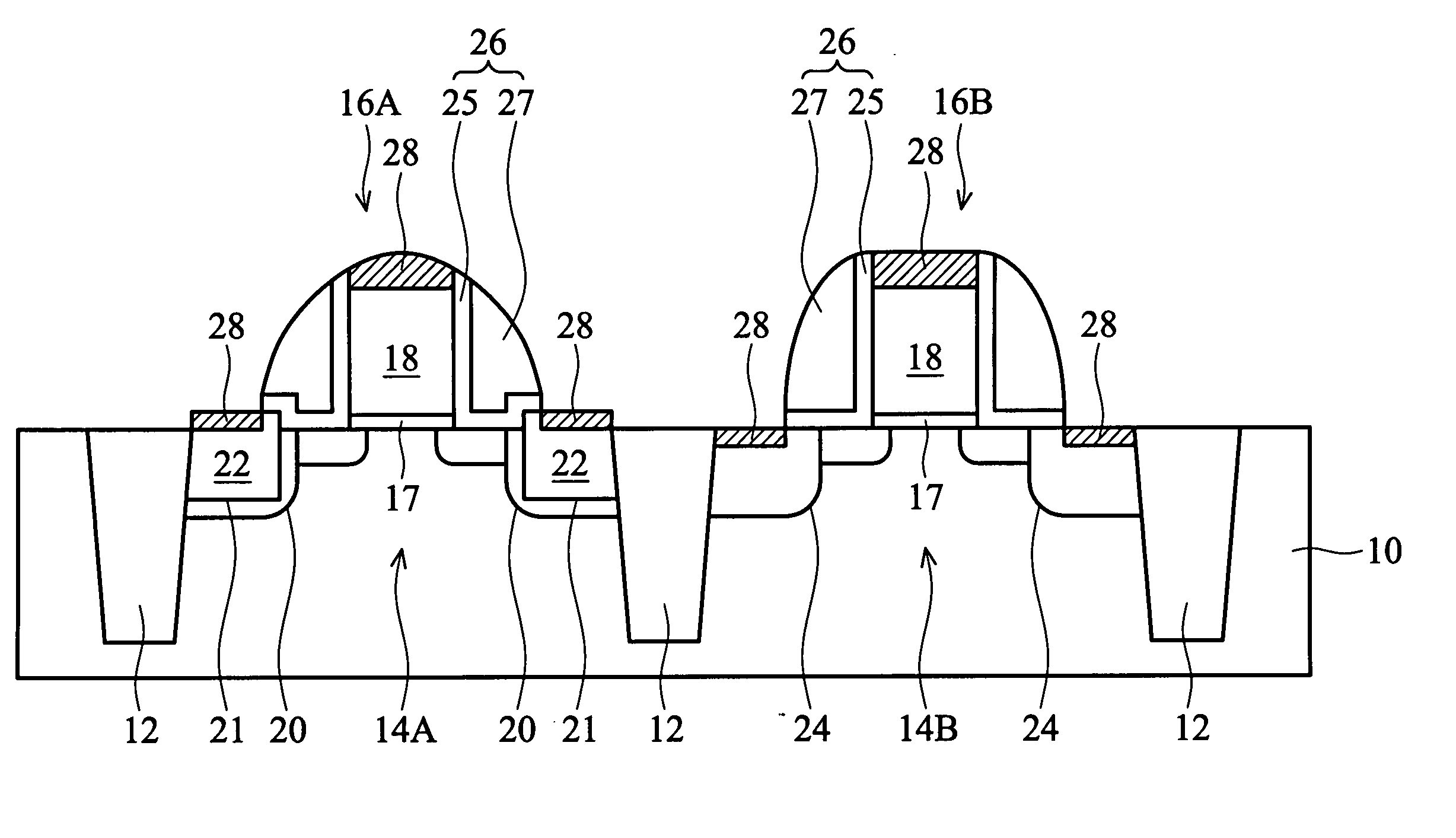
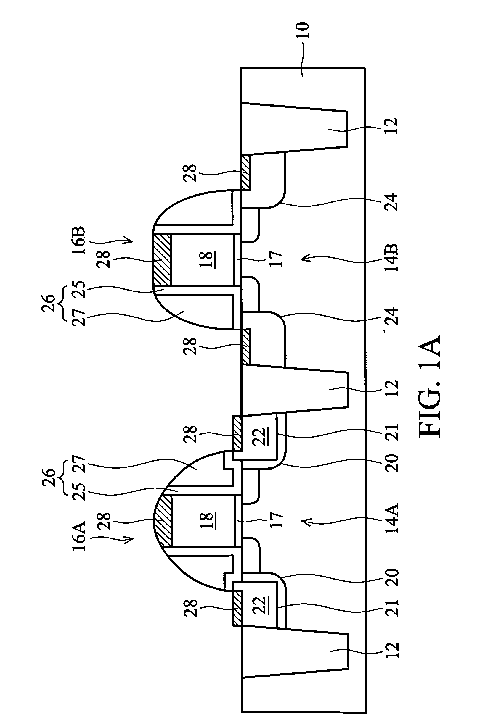
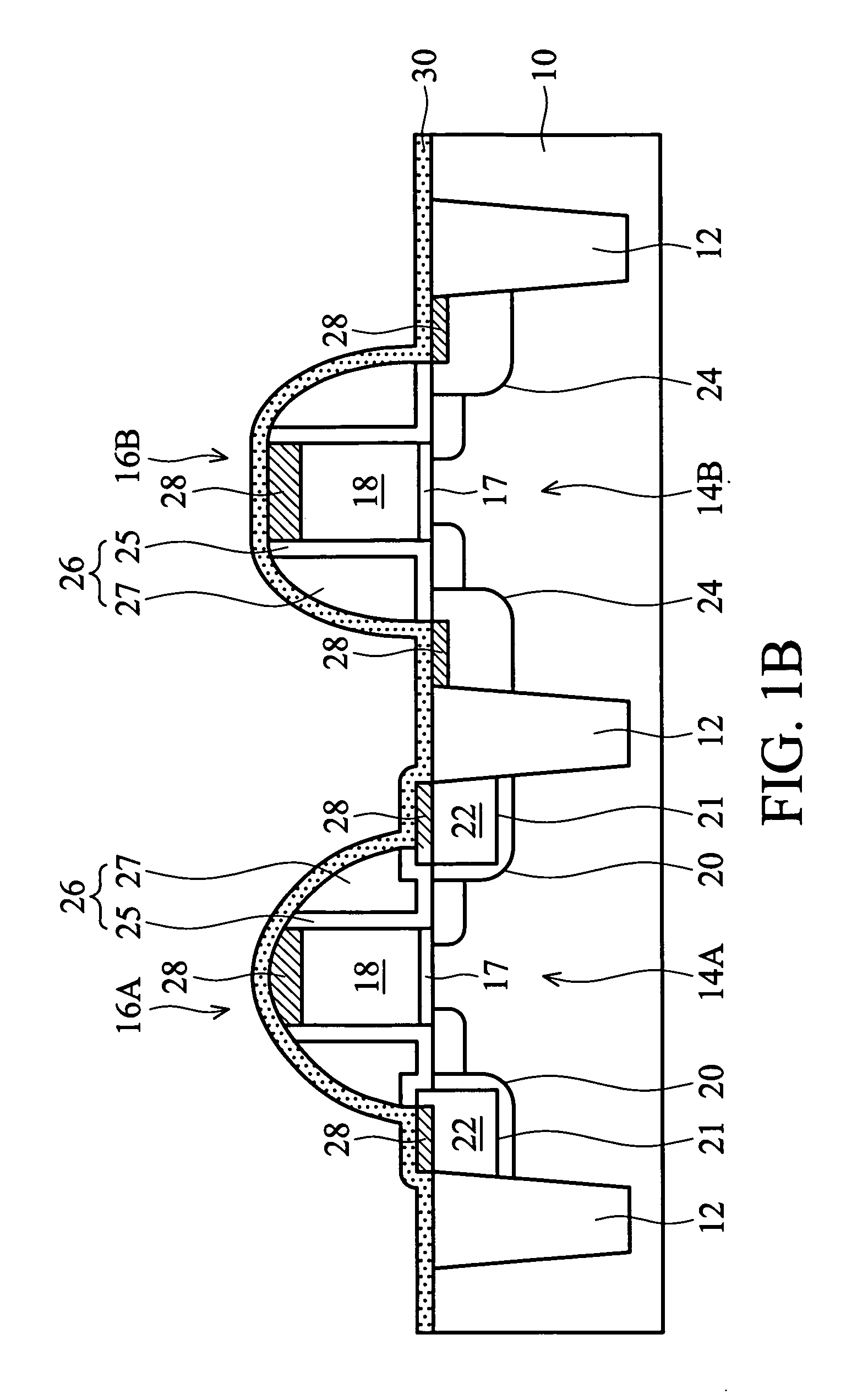
[0016] Embodiments of the present invention provide strain enhanced CMOS devices using amorphous carbon films and fabrication methods of forming the same, which overcome the aforementioned problems of the prior art through the use of SiN capping films. The amorphous carbon (a-C) film, such as a fluorinated amorphous carbon (a-C:F) film, is a low-temperature deposition material formed by chemical vapor deposition (CVD) or physical vapor deposition (PVD). The amorphous carbon film has low dielectric constant. For example, a-C:F has a k value less than 2.8. Depending on deposition conditions (e.g., power, temperature, and the like), the amorphous carbon film may be formed of a tensile film or a compressive film to act a stress capping film that may be selectively formed on a pMOS device region and / or an nMOS device region. The amorphous carbon film may also act a contact etching stop layer (CESL) because of its good selectivity to oxide, nitride and silicide, thus the problems caused b...


PUM

PropertyMeasurementUnit
dielectric constantaaaaaaaaaa
thicknessaaaaaaaaaa
dielectric constantaaaaaaaaaa

Abstract

A strain enhanced CMOS device using amorphous carbon films and fabrication methods of forming the same. The amorphous carbon (a-C) film, such as fluorinated amorphous carbon (a-C:F), is formed of a tensile film or a compressive film to act a stress capping film on the pMOS device region or the nMOS device region. The amorphous carbon film also acts a contact etching stop layer during a contact hole etching process.

Description

TECHNICAL FIELD [0001] The present invention relates to CMOS devices in integrated circuit manufacturing processes, and more particularly to strain enhanced CMOS devices using amorphous carbon films and fabrication methods of forming the same. BACKGROUND [0002] A principal factor in maintaining adequate performance in field effect transistors (FETs) is carrier mobility that affects the amount of current or charge in a doped semiconductor channel under control of a voltage placed on a gate electrode insulated from the channel by a very thin dielectric. Reduced carrier mobility in an FET reduces not only the switching speed of a given transistor but also the difference between “on” resistance and “off” resistance. Particularly, in the development of complementary metal-oxide-semiconductor (CMOS) field effect transistors, carrier mobility is a design concern. One problem facing CMOS manufacturing is that nMOS and pMOS devices require different types of stress in order to achieve increa...

Claims


Application Information

Patent Timeline
Patent Type & Authority Applications(United States)
IPC IPC(8): H01L29/94H01L21/8238
CPCH01L21/823807H01L29/7843H01L29/665H01L21/823864
Inventor CHEN, CHENG-KU
Owner TAIWAN SEMICON MFG CO LTD
Why Eureka
Try Eureka