

Varnish Containing Good Solvent And Poor Solvent
- Summary
- Abstract
- Description
- Claims
- Application Information
AI Technical Summary
Benefits of technology
Problems solved by technology
Method used
Image

Examples
example 1
[0146] Phenyltetraaniline (hereinafter abbreviated as “PTA”) represented by the formula (7) was synthesized from p-hydroxydiphenylamine and p-phenylenediamine in accordance with Bulletin of Chemical Society of Japan, 67, 1749-1752 (1994) (yield: 85%).
[0147] [Chemical Formula 12]
[0148] The resultant PTA (0.0500 g, 0.1130 mmol) and 5-sulfosalicylic acid (5-SSA) represented by the formula (8) (product of Wako Pure Chemical Industries, Ltd.; 0.0986 g, 0.4520 mmol)) were completely dissolved in 1,3-dimethyl-2-imidazolidinone (DMI, 5.8846 g) under a nitrogen atmosphere.
[0149] [Chemical Formula 13]
[0150] To the thus-obtained solution, cyclohexanol (c-HexOH, 8.8268 g) was added, followed by stirring to prepare a charge-transporting varnish (solid content: 1.0%).
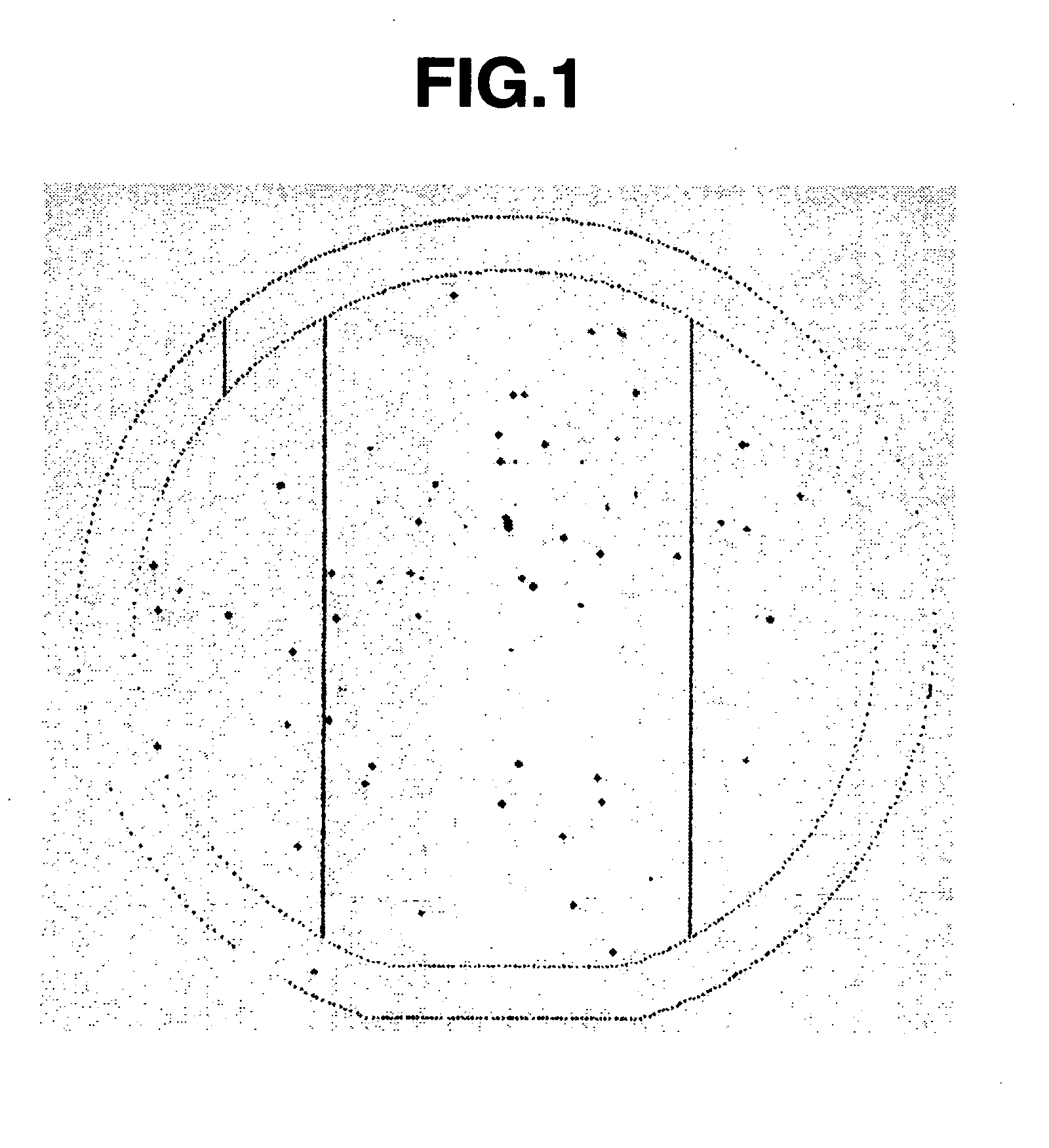
[0151]FIG. 1 illustrates the results of an inspection and measurement of surface contamination particles on a charge-transporting thin film obtained by forming a varnish of Example 1 into a film on a silicon wafer and baking the s...
example 2
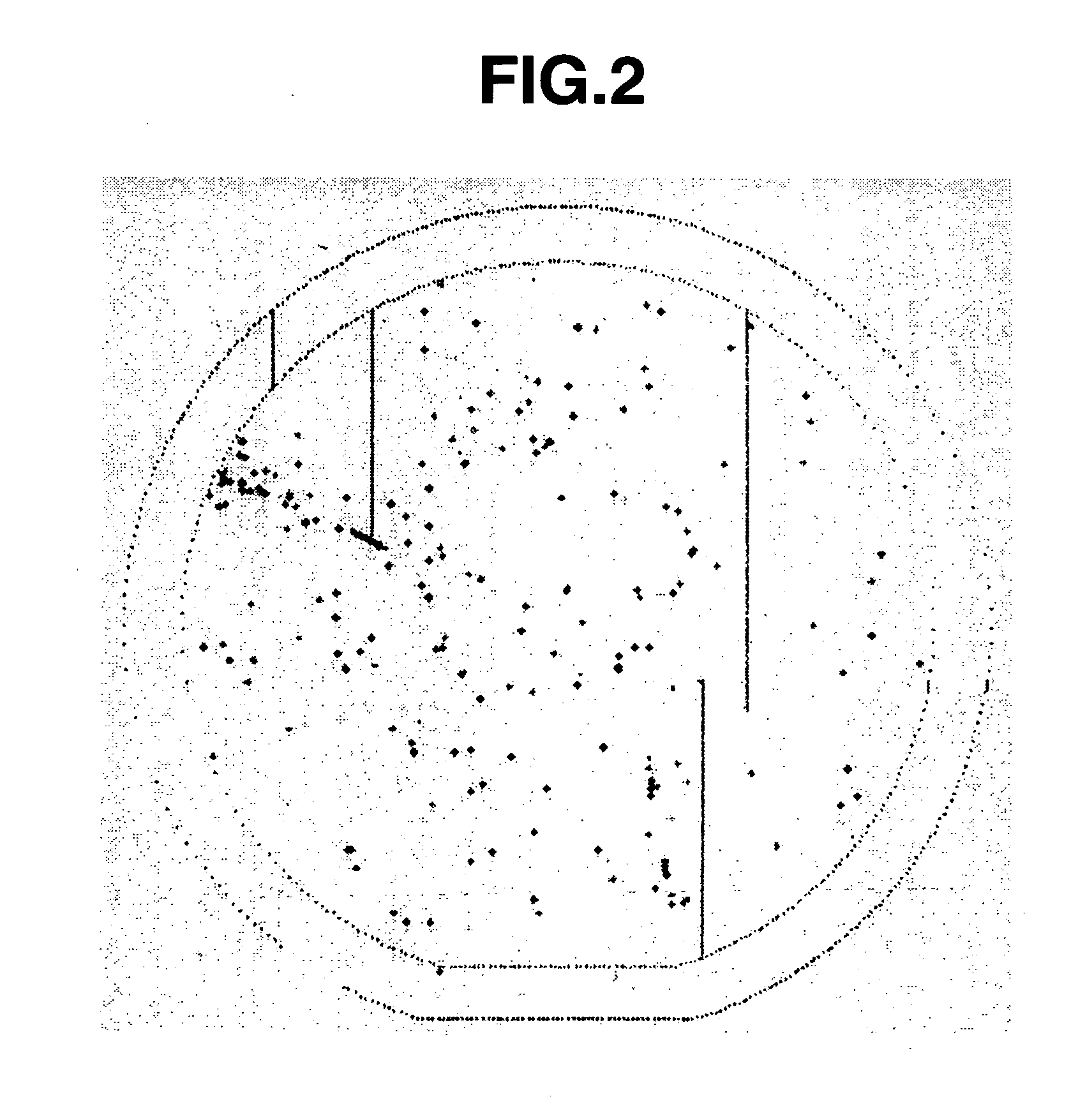
[Example 2]
[0158] In a similar manner as in Example 1, PTA (0.1000 g, 0.2260 mmol) and 5-SSA (0.1972 g, 0.9040 mmol) were completely dissolved in DMI (4.1775 g) under a nitrogen atmosphere.
[0159] To the thus-obtained solution, c-HexOH (6.2662 g) was added, followed by stirring to prepare a charge-transporting varnish (solid content: 3.0%).
example 3
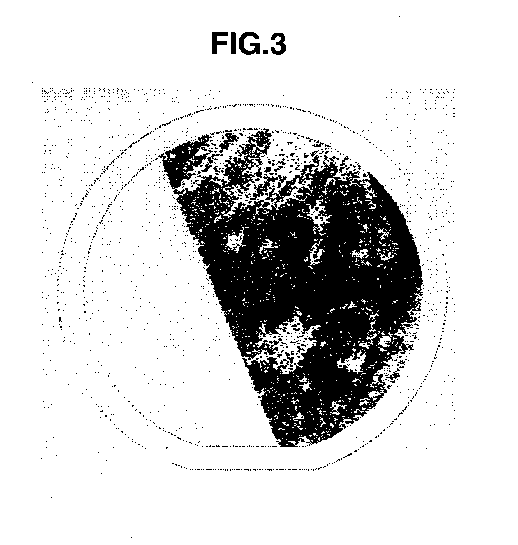
[0160] In a similar manner as in Example 1, PTA (0.1000 g, 0.2260 mmol) and 5-SSA (0.1972 g, 0.9040 mmol) were completely dissolved in N-methylpyrrolidone (4.1775 g) under a nitrogen atmosphere.
[0161] To the thus-obtained solution, c-HexOH (6.2662 g) was added, followed by stirring to prepare a charge-transporting varnish (solid content: 3.0%).
PUM
| Property | Measurement | Unit |
|---|---|---|
| Fraction | aaaaa | aaaaa |
| Fraction | aaaaa | aaaaa |
| Length | aaaaa | aaaaa |
Abstract
Description
Claims
Application Information