Nitride semiconductor device and process for producing the same

a technology of semiconductor laser devices and nitride, which is applied in the direction of semiconductor lasers, lasers, coatings, etc., can solve the problems of difficult to obtain highly reliable semiconductor laser devices, including dislocations, etc., and achieves improved reliability and producibility, good yield, and low resistance

Active Publication Date: 2007-09-20
PANASONIC CORP
View PDF7 Cites 31 Cited by
  • Summary
  • Abstract
  • Description
  • Claims
  • Application Information

AI Technical Summary

Benefits of technology

[0047] According to the present invention, a nitride semiconductor having a small dislocation density can be fabricated with a good yield, and the operating voltage of a nitride semiconductor device having electrodes provided on the rear face of its substrate can be reduced while also attaining improved reliability and producibility.
[0048] Moreover, according to the present invention, even when the nitride semiconductor layer is doped with an n-type impurity at a high concentration so as to realize low resistance, cracks can be suppressed, the operating voltage of the nitride semiconductor device can be reduced, and an improved reliability and producibility can be obtained. As a result, a highly-reliable laser for optical disks, laser display apparatus, and laser for medical use can be fabricated with a good yield.

Problems solved by technology

A GaN substrate which has been fabricated by the above method has a problem in that it includes dislocations, e.g., edge dislocations, screw dislocations, and mixed dislocations, at a density of about 5×107 cm−2.
When dislocations are present at such a large density, it is difficult to obtain a highly-reliable semiconductor laser device.

Method used


Image

  • Nitride semiconductor device and process for producing the same
  • Nitride semiconductor device and process for producing the same
  • Nitride semiconductor device and process for producing the same

Examples


embodiment 1

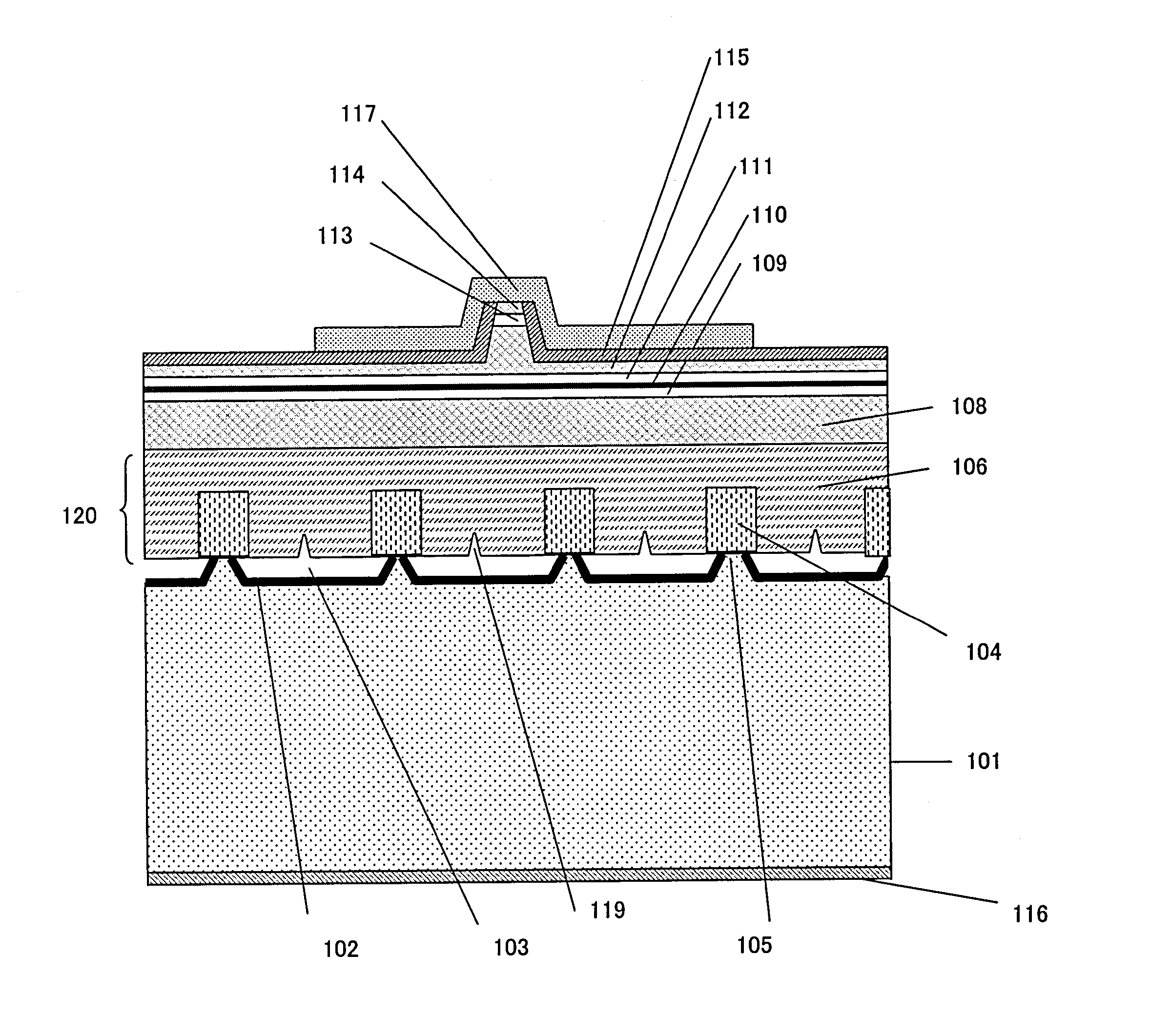
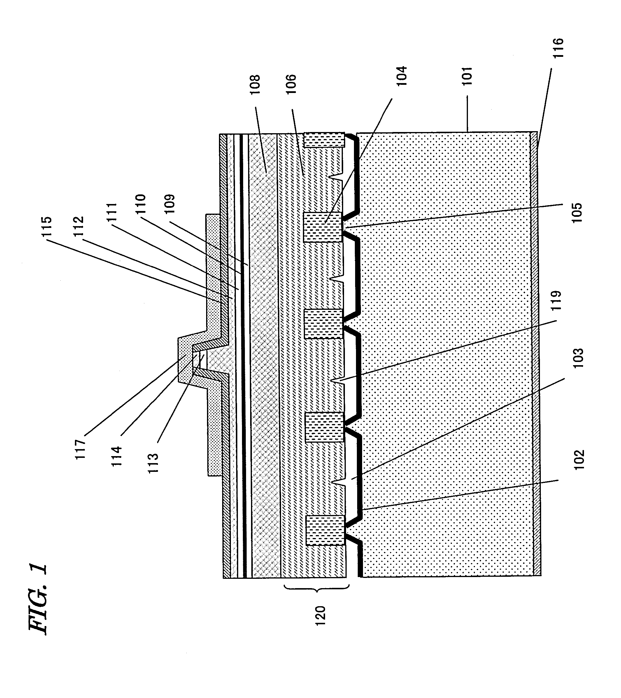
[0111] First, FIG. 1 is referred to. FIG. 1 shows a cross section of a nitride semiconductor laser device according to the present embodiment. The semiconductor laser device of the present embodiment includes an n-GaN substrate 101 having a plurality of stripe ridges formed on its principal face, and a semiconductor multilayer structure grown on the n-GaN substrate 101 substrate. Portions of the principal face of the n-GaN substrate 101 other than the upper faces of the stripe ridges are covered by a mask layer 102 which is composed of SiNx (0105 having a crystal surface which is parallel to the principal face of the substrate, and depressions are formed between the stripe ridges. The depressions are not buried with any semiconductor layer or the like, and air gaps 103 exist between the principal face of the n-GaN substrate 101 and the bottom face of the semiconductor multilayer structure.

[0112] In the present embodiment, AlxGayInzN crystals (x=0 y=1 z=0) which contain an n-type im...

embodiment 2

[0149] Next, with reference to FIGS. 17(a) to (d), a second embodiment of the present invention will be described.

[0150] Main differences between the present embodiment and Embodiment 1 described above are the surface orientation of the n-GaN substrate 101 and the step of forming the nitride semiconductor layer 120. Therefore, only these differences will be described in detail below.

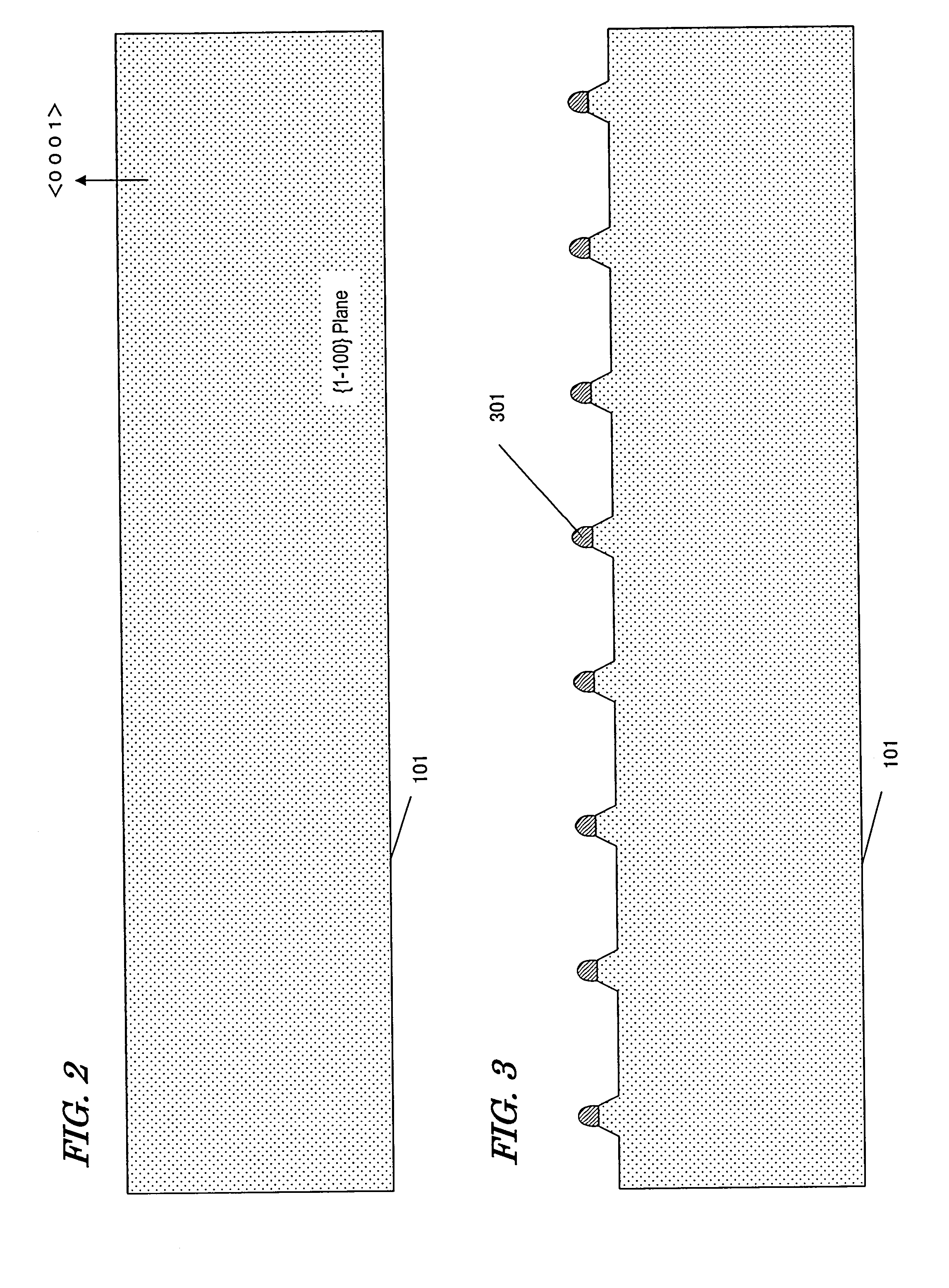
[0151] First, in a step similar to the step described with respect to the above-described embodiment, the n-GaN substrate 101 shown in FIG. 17(a) is provided. However, a normal direction of the principal face of the GaN substrate 101 used in the present embodiment is , instead of . On the principal face of the GaN substrate 101, stripe ridges which are parallel to are formed.

[0152] Next, as shown in FIG. 17(b), first n-GaN crystals 1401 are grown on seeds 105 of the GaN substrate 101 by MOVPE technique. At this time, by adjusting the growth conditions such as temperature and the V / III ratio during th...

embodiment 3

[0162] Hereinafter, with reference to FIG. 19, a third embodiment of the present invention will be described.

[0163] The present embodiment differs from Embodiment 1 largely in that after growing the second n-GaN crystal 106 and before forming the n-Al0.1Ga0.9N / GaN superlattice cladding layer 108, an n-Al0.1Ga0.9N / GaN superlattice contact layer 107 is formed on the second n-GaN crystal 106, and that a p electrode and an n electrode are provided on the same face of the GaN substrate. Otherwise, the construction is similar to the construction of Embodiment 1, and no detailed descriptions will be repeated of the constituent elements which are common to these embodiments.

[0164] In the present embodiment, after stacking the n-Al0.1Ga0.9N / GaN superlattice cladding layer 108, the n-GaN optical guide layer 109, the multi-quantum well (MQW) active layer 110, the p-GaN optical guide layer 111, the p-Al0.1Ga0.9N / GaN cladding layer 112, and the p-GaN layer 113 on the n-Al0.1Ga0.9N / GaN superlat...


PUM

PropertyMeasurementUnit
widthaaaaaaaaaa
widthaaaaaaaaaa
widthaaaaaaaaaa

Abstract

A process for producing a nitride semiconductor according to the present invention includes: step (A) of provided an n-GaN substrate 101; step (B) of forming on the substrate 101 a plurality of stripe ridges having upper faces which are parallel to a principal face of the substrate 101; step (C) of selectively growing AlxGayInzN crystals (0≦x, y, z≦1: x+y+z=1) 104 on the upper faces of the plurality of stripe ridges, the AlxGayInzN crystals containing an n-type impurity at a first concentration; and step (D) of growing an Alx<sup2>′</sup2>Gay<sup2>′</sup2>Inz<sup2>′</sup2>N crystal (0≦x′, y′, z′≦1: x′+y′+z′=1) 106 on the AlxGayInzN crystals 104, the Alx<sup2>′</sup2>Gay<sup2>′</sup2>Inz<sup2>′</sup2>N crystal 106 containing an n-type impurity at a second concentration which is lower than the first concentration, and linking every two adjoining AlxGayInzN crystals 104 with the Alx<sup2>′</sup2>Gay<sup2>′</sup2>Inz<sup2>′</sup2>N crystal 106 to form one nitride semiconductor layer 120.

Description

TECHNICAL FIELD [0001] The present invention relates to a nitride semiconductor device such as a semiconductor laser device and a light-emitting diode, and a process for producing the same. BACKGROUND ART [0002] Blue / violet semiconductor laser devices which are fabricated by using III-V group nitride-type semiconductor materials such as gallium nitride are key devices for realizing ultra-high density recording with optical disk apparatuses, and are about to reach a practical level. Increases in the output power of blue / violet semiconductor laser devices not only make possible a fast write to optical disks, but also open doors to new fields of technology, such as application to laser displays. [0003] Conventionally, GaN-type semiconductor laser devices employing sapphire substrates have been developed. In recent years, however, use of nitride semiconductor substrates, e.g., GaN substrates, for fabricating GaN-type semiconductor laser devices has been studied. For example, Non-Patent ...

Claims


Application Information

Patent Timeline
Patent Type & Authority Applications(United States)
IPC IPC(8): H01S5/30H01L21/20C23C16/34H01L21/205H01L33/00H01S5/22H01S5/32H01S5/323H01S5/343
CPCB82Y20/00H01S2304/12H01L21/02458H01L21/0254H01L21/02636H01L21/02639H01L21/02642H01L21/0265H01L33/0075H01S5/2201H01S5/305H01S5/3216H01S5/34333H01S2301/173H01S2304/04H01L21/02389
Inventor ISHIBASHI, AKIHIKOYOKOGAWA, TOSHIYASHIMAMOTO, TOSHITAKAHASEGAWA, YOSHIAKIKAWAGUCHI, YASUTOSHIKIDOGUCHI, ISAO
Owner PANASONIC CORP
Why Eureka
Try Eureka