Method for reducing metal, multilayer interconnection structure and manufacturing method for the same, and semiconductor device and manufacturing method for the same

a technology of multilayer interconnection structure and manufacturing method, applied in semiconductor/solid-state device manufacturing, basic electric elements, electric apparatus, etc., can solve the problems of reducing signal propagation speed, and less effect of interconnection delay on the whole of the semiconductor device, so as to reduce parasitic capacity, reduce interconnection resistance, and increase the permittivity of the insulating film

Inactive Publication Date: 2007-09-27
FUJITSU SEMICON LTD
View PDF20 Cites 1 Cited by
  • Summary
  • Abstract
  • Description
  • Claims
  • Application Information

AI Technical Summary

Benefits of technology

[0027]In this semiconductor device, oxidized metal on the interconnections is reduced to metal using the metal reduction method of the present invention. Accordingly, this semiconductor device is allowed to include a multilayer interconnection structure having reduced interconnection resistance without increasing the permittivity of the insulating film; therefore, it is possible to achieve reduced parasitic capacities between interconnections and reduced interconnection resistance. Thus, the semiconductor device of the present invention is particularly suitable, for example, for flash memories, DRAMs, FRAMs and MOS transistors, which are high-speed and highly reliable.
[0028]The method of the present invention for manufacturing a semiconductor device is characterized by including at least a film formation step of forming a film on a work surface, a patterning step of patterning the work surface by an etching process using the film as a mask, an interconnection formation step of forming an interconnection on the work surface, and a reduction step of subjecting the surface of the interconnection formed on the work surface to reduction treatment using the metal reduction method of the present invention. With this manufacturing method, a film is formed on a work surface, where a multilayer interconnection structure is to be formed, using a film formation material in the film formation step, the work surface is patterned by an etching process using the film as a mask in the

Problems solved by technology

Conventionally, it has been known that increased parasitic capacities in insulating films cause a reduction in signal propagation speed.
In a semiconductor device with an interconnection pitch of as large as 1 μm or more, however, interconnection delay has less effect on the whole of the semiconductor device.
Because both the interconnection resistance and parasitic capacities between interconne

Method used


Image

  • Method for reducing metal, multilayer interconnection structure and manufacturing method for the same, and semiconductor device and manufacturing method for the same
  • Method for reducing metal, multilayer interconnection structure and manufacturing method for the same, and semiconductor device and manufacturing method for the same
  • Method for reducing metal, multilayer interconnection structure and manufacturing method for the same, and semiconductor device and manufacturing method for the same

Examples


example 1

Reduction Treatment>

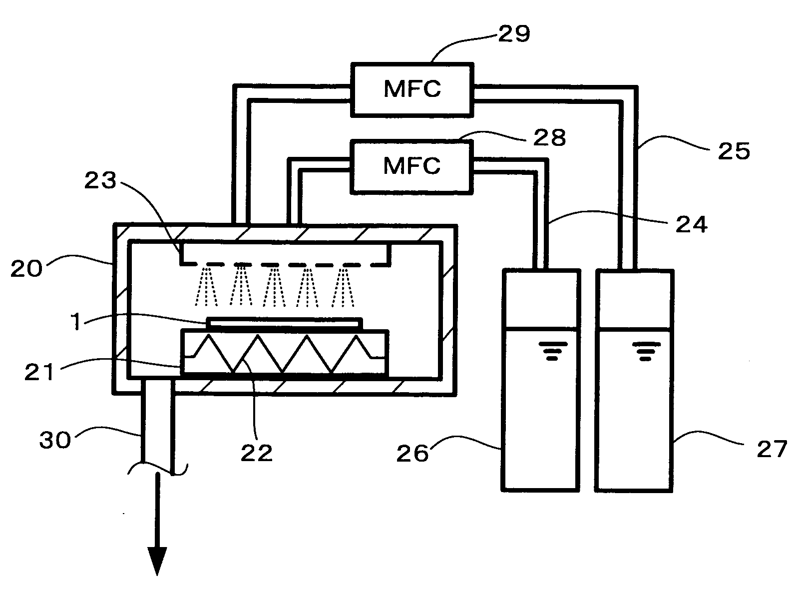
[0148]A silicon wafer 1 provided with the foregoing porous silica film was placed on a support board 21 in a chamber 20 of a metal reduction apparatus as shown in FIG. 1. Subsequently, a reduction source (ethyl formate) and a hydrolysis source (water) were heated to temperatures described below, vaporized, and introduced in the chamber 20 at flow rates described below. In this way the porous silica film on the silicon wafer 1 was exposed to the reduction treatment environment described below. Note that the substrate temperature described below indicates the temperature of the silicon wafer 1 heated by a heater 22 provided in the chamber 20.

-Reduction Source-

[0149]Source: Ethyl formate

[0150]Source heating temperature: 80° C.

[0151]Flow rate: 400 sccm

Hydrolysis Source

[0152]Source: Water

[0153]Source heating temperature: 80° C.

[0154]Flow rate: 100 sccm

Exposure Atmosphere

[0155]Substrate temperature: 250° C.

[0156]Pressure in chamber: 100 Pa

[0157]Treatment time: 180 seco...

example 2

[0159]A porous silica film on a silicon wafer, obtained in a manner similar to that described above, was exposed to the reduction treatment atmosphere of Example 2 using a metal reduction apparatus similar to that of Example 1, shown in FIG. 1, in a manner similar to that described in Example 1 except that the reduction source was changed to the species described below.

-Reduction Source-

[0160]Source: Ethyl acetate

[0161]Source heating temperature: 80° C.

[0162]Flow rate: 400 sccm

-Hydrolysis Source-

[0163]Source: Water

[0164]Source heating temperature: 80° C.

[0165]Flow rate: 100 sccm

-Exposure Atmosphere-

[0166]Substrate temperature: 250° C.

[0167]Pressure in chamber: 100 Pa

[0168]Treatment time: 180 seconds

[0169]After exposing the porous silica film to such an environment, permittivity was measured in a manner similar to that used for the measurement before the exposure treatment; permittivity was not changed from 2.3.

example 3

[0170]A porous silica film on a silicon wafer, obtained in a manner similar to that described above, was exposed to the reduction treatment atmosphere of Example 3 using a metal reduction apparatus similar to that of Example 1, shown in FIG. 1, in a manner similar to that described in Example 1 except that the reduction source was changed to the species described below.

-Reduction Source-

[0171]Source: Methyl propionate

[0172]Source heating temperature: 80° C.

[0173]Flow rate: 400 sccm

-Hydrolysis Source-

[0174]Source: Water

[0175]Source heating temperature: 80° C.

[0176]Flow rate: 100 sccm

-Exposure Atmosphere-

[0177]Substrate temperature: 250° C.

[0178]Pressure in chamber: 100 Pa

[0179]Treatment time: 180 seconds

[0180]After exposing the porous silica film to such an environment, permittivity was measured in a manner similar to that used for the measurement before the exposure treatment; permittivity was not changed from 2.3.


PUM

PropertyMeasurementUnit
Temperatureaaaaaaaaaa

Abstract

To provide a reliable, efficient method for reducing oxidized metals used upon manufacturing of the multilayer interconnection structure, semiconductor device, etc. With this method vapor containing at least a carboxylic acid ester is hydrolyzed by water vapor to reduce oxidized metal. The multilayer interconnection manufacturing method of the present invention includes at least film formation step, interconnection formation step, and reduction step using the metal reduction method of the present invention. The multilayer interconnection structure of the present invention is manufactured by the multilayer interconnection structure manufacturing method of the present invention. The semiconductor device manufacturing method of the present invention includes at least film formation step, patterning step, interconnection formation step, and reduction step using the metal reduction method. The semiconductor device of the present invention includes at least multilayer interconnection structure of the present invention and is formed using the semiconductor device manufacturing method of the present invention.

Description

CROSS-REFERENCE TO RELATED APPLICATIONS[0001]This application is based upon and claims the benefits of the priority from the prior Japanese Patent Application No. 2006-083864 filed on Mar. 24, 2006, the entire contents of which are incorporated herein by reference.BACKGROUND OF THE INVENTION[0002]1. Field of the Invention[0003]The present invention relates to a reliable, efficient method for reducing oxidized metal; a multilayer interconnection structure with reduced interconnection resistance where parasitic capacities between interconnections can be reduced with the method, and an efficient method for manufacturing the same; and a high-speed, highly-reliable semiconductor device having the multilayer interconnection structure, and an efficient method for manufacturing the same. More particularly, the present invention relates to a method for reducing copper oxide for reducing copper interconnections efficiently, reliably and inexpensively during the formation of a multilayer inter...

Claims


Application Information

Patent Timeline
IPC IPC(8): C25C3/00
CPCH01L21/02063H01L21/76807H01L21/76835H01L21/76829H01L21/76834H01L21/76814H01L21/28C22B5/02C22B5/12C22B5/10
Inventor NAKATA, YOSHIHIRO
Owner FUJITSU SEMICON LTD
Why Eureka
Try Eureka