Electronic Package Formed Using Low-Temperature Active Solder Including Indium, Bismuth, and/or Cadmium

a technology of active solder and electronic components, which is applied in the direction of solid-state devices, machines/engines, metal-working apparatuses, etc., can solve the problems of flux residues remaining on the soldered workpiece surface, complex operation of the soldering operation, and high risk, and achieve high-temperature conductivity joints and high-strength

Inactive Publication Date: 2007-10-04
S BOND TECH
View PDF23 Cites 50 Cited by
  • Summary
  • Abstract
  • Description
  • Claims
  • Application Information

AI Technical Summary

Benefits of technology

[0017] The invention encompasses an active solder alloy, an electronic device package including the active solder alloy bonding an electronic device to a substrate, and a method of forming high-strength, high-thermal conductivity joints by soldering using the solder alloy. The alloy contains up to about 10% by weight of an element or a mixture of elements selected from the group consisting of titanium, zirconium, hafnium, vanadium, niobium, or tantalum; between about 0.1 and 5% by weight of an element or a mixture of elements selected from the group of the l

Problems solved by technology

These limitations mean that the workpiece surfaces to be soldered require a complicated pretreatment, that the soldering operation is made more complex by the use of added flux, or both.
In addition, the risk exists that, after the soldering process, flux residues will remain on the soldered workpiece surfaces.
Residual flux may cause problems in further processing steps or impair the long-term durability of the soldered joints.
Some of these conventional soldering processes are hazardous to health, the environment, or both.
Other commercial soldering processes use soft solder alloys, which comprise tin and/or lead and possibly silver, and have a process temperature of about 180-280° C. Such processes have the further limitation that they wet many materials either not at all or only very poorly.
Therefore, these processes cannot be used to join workpieces made of poorly wettable or entirely nonwettable materials such as ceramics.
A significant limitation of the processes using active solders is, however, that they require process temperatures between 600° C. to 900° C. and require a protective atmosphere such as a high vacuum or a pure shielding gas.
The high processing temperature severely limits the choice of solderable materials.
Furthermore, the need for a vacuum or shielding gas complicates the soldering operation and, in many cases, precludes application of the process at all.
(at 233° C.

Method used


Image

  • Electronic Package Formed Using Low-Temperature Active Solder Including Indium, Bismuth, and/or Cadmium
  • Electronic Package Formed Using Low-Temperature Active Solder Including Indium, Bismuth, and/or Cadmium
  • Electronic Package Formed Using Low-Temperature Active Solder Including Indium, Bismuth, and/or Cadmium

Examples


Embodiment Construction

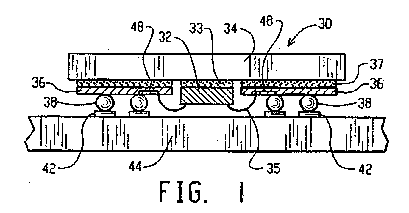
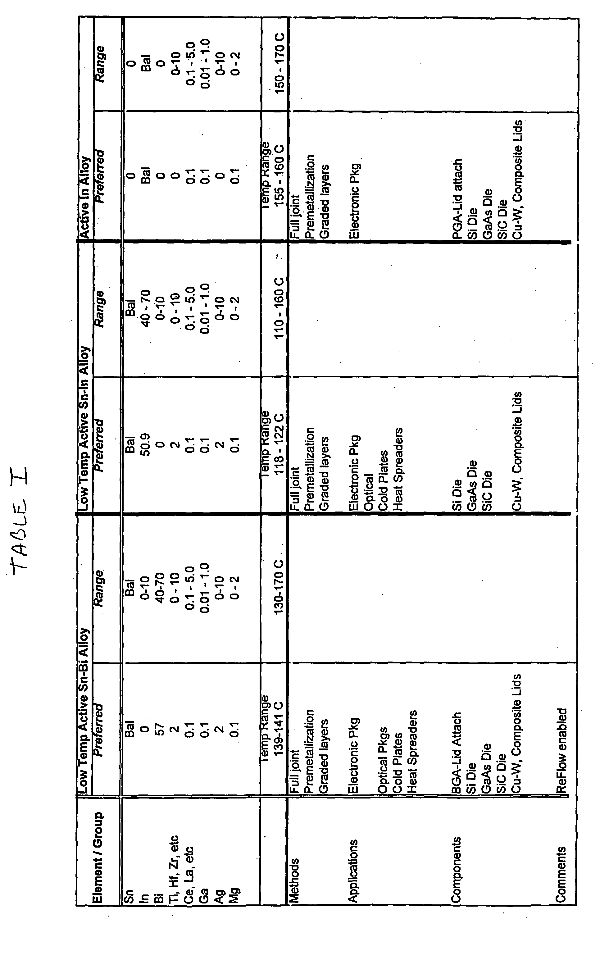
[0021] This patent application describes a series of lower-temperature active solders to for use in electronic packaging. The reason to create lower temperature active solders, in contrast to the known active solder compositions (e.g., the Sn—Ag—Ti—Ga—Ce composition taught by U.S. Pat. No. 6,231,693 issued to Lugscheider et. al.), lies in the need to join at temperatures below 220° C. and even more importantly below 183° C. This latter temperature is the eutectic melting temperature for the Pb—Sn solders that are still being used as solder interconnects in direct mount, ball grid arrays (BGA's).

[0022] A solubility curve defines the solubility limit (maximum solute addition without supersaturation) of a solid in a liquid. The point at which two solubility curves intersect in a phase or equilibrium diagram (a map from which the phases present at any particular temperature or composition can be read if the alloy is at equilibrium, i.e., if all possible reaction has been completed) def...


PUM

PropertyMeasurementUnit
Temperatureaaaaaaaaaa
Percent by massaaaaaaaaaa

Abstract

An active solder alloy, an electronic device package including the active solder alloy bonding an electronic device to a substrate, and a method of forming high-strength joints by soldering using the solder alloy. The alloy contains up to about 10% by weight of an element or a mixture of elements selected from the group consisting of titanium, zirconium, hafnium, vanadium, niobium, or tantalum; between about 0.1 and 5% by weight of an element or a mixture of elements selected from the group of the lanthanides (rare earths); between about 0.01 and 1% by weight of gallium up to about 10% by weight of silver; up to about 2% by weight of magnesium; and a remainder consisting of tin, bismuth, indium, cadmium, or a mixture of two or more of these elements. The alloy enables low-temperature (less than about 180° C.) soldering within relatively narrow melting ranges (less than about 10° C.).

Description

RELATED APPLICATION [0001] This application claims the benefit of priority to U.S. Provisional Patent Application No. 60 / 568,037 titled “Low-Temperature Active Solder Including Indium, Bismuth, And / Or Cadmium,” filed on May 4, 2004, and to U.S. Provisional Patent Application No. 60 / 643,640 titled “Use of Active Solder Compositions in Electronic Packaging,” filed on Jan. 13, 2005, the contents of which are incorporated in this application by reference.TECHNICAL FIELD [0002] The present invention relates generally to an electronic package formed using a solder alloy and, more particularly, to an active solder alloy composition including active and other elements that permit fluxless solder joining of workpieces below 180° C. The invention also includes a method for joining ceramics and other applications that benefit from the composition. BACKGROUND OF THE INVENTION [0003] The process of soldering is one of the most widely used joining techniques. Even wider use of soldering for joini...

Claims


Application Information

Patent Timeline
IPC IPC(8): B23K35/26B23K1/00C22C12/00C22C13/00C22C28/00B23K1/06B23K1/20H01L23/485
CPCB23K35/262B23K35/264H01L24/13H01L2224/48227H01L2224/32245H01L2924/10253H01L2924/014H01L2924/01072H01L2924/0107H01L2924/01068H01L2924/01047B23K35/266C22C12/00C22C13/00C22C28/00H01L24/10H01L2224/13099H01L2224/48091H01L2224/73265H01L2924/01012H01L2924/01013H01L2924/01022H01L2924/01029H01L2924/0104H01L2924/01042H01L2924/01046H01L2924/01049H01L2924/01057H01L2924/01058H01L2924/01059H01L2924/01064H01L2924/01073H01L2924/01074H01L2924/01075H01L2924/01078H01L2924/01079H01L2924/01082H01L2924/01105H01L2924/01322H01L2924/10329H01L2924/14H01L2924/15153H01L2924/1517H01L2924/15311H01L2924/1532H01L2924/3025H01L2224/13109H01L2924/01005H01L2924/01006H01L2924/01019H01L2924/01023H01L2924/01033H01L2924/01041H01L2924/00014H01L2924/00H01L2924/00012H01L2924/12042H01L24/73H01L2224/13B23K1/06B23K1/20H01L23/485
Inventor SMITH, RONALD W.REDD, RANDALL
Owner S BOND TECH
Why Eureka
Try Eureka