Etching reagent, and method for manufacturing electronic device substrate and electronic device

a technology of electronic devices and etching reagents, which is applied in the direction of basic electric elements, transistors, chemistry apparatuses and processes, etc., can solve the problems of difficult to control the immersion time of cu films, difficult to obtain cu wiring having a desired line width, and slimming phenomenon

Inactive Publication Date: 2007-10-11
LG DISPLAY CO LTD
View PDF3 Cites 13 Cited by
  • Summary
  • Abstract
  • Description
  • Claims
  • Application Information

AI Technical Summary

Benefits of technology

[0013] Accordingly, the object of the present invention carried out in view of the foregoing circumstances is to provide an etching agent that enables the Cu film to be etched by a simple chemical etching method such as a stationary immersion method for using a low resistance Cu film as a wiring material with little time dependent change of the etching rate, besides preventing the pattern slimming phenomenon caused by irregular amount of etching at the side face of the Cu film (the amount of side etching).

Problems solved by technology

When a mixed solution of acetic acid and hydrogen peroxide or a ammonium peroxosulfate solution is used as an etching agent, it is difficult to control the immersion time of the Cu film since the etching rate is vigorously changed with time, thereby making it difficult to obtain a Cu wiring having a desired line width.
However, the slimming phenomenon as described above is not observed when the acetic acid-hydrogen peroxide based etching agent is used.

Method used


Image

  • Etching reagent, and method for manufacturing electronic device substrate and electronic device
  • Etching reagent, and method for manufacturing electronic device substrate and electronic device
  • Etching reagent, and method for manufacturing electronic device substrate and electronic device

Examples


first embodiment

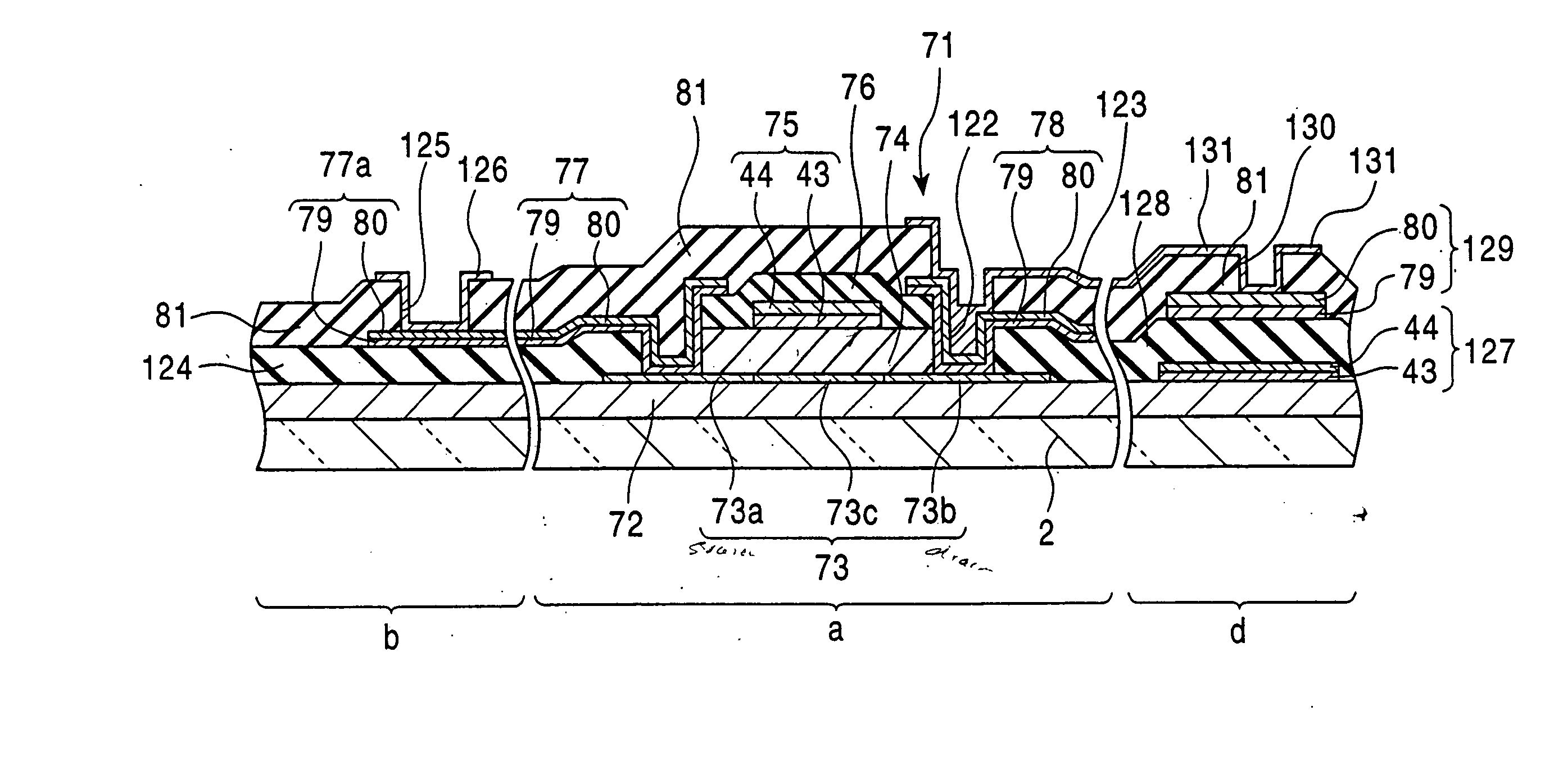
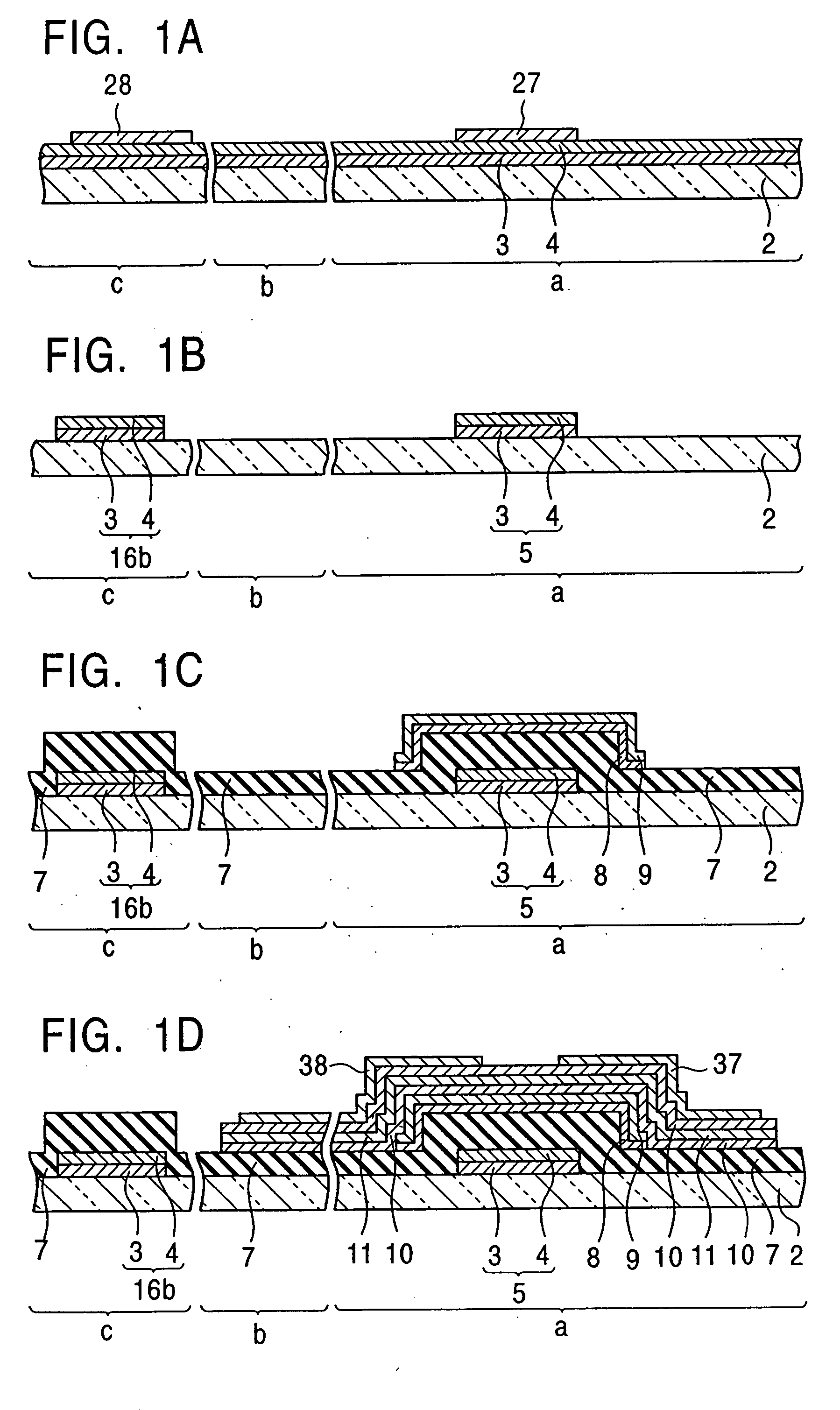
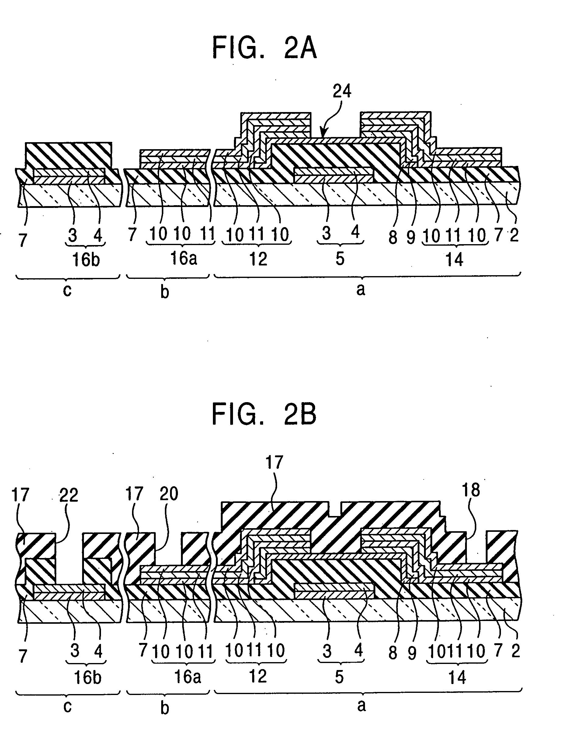
[0060]FIG. 3 is a partial cross section showing an example of the thin film transistor substrate manufactured by applying the method for manufacturing the electronic device substrate according to the present invention to a method for manufacturing a thin film transistor substrate (the method for manufacturing the thin film transistor substrate according to the first embodiment) provided in a liquid crystal display device.

[0061] The portions with reference marks a, b and c denote a thin film transistor portion (TFT), a terminal portion of a source wiring located at outside of a TFT matrix and a terminal portion of a gate wiring, respectively. Although these three portions are located with some distances apart in the actual liquid crystal device provided with this thin film transistor substrate 1, and they can not be naturally exhibited simultaneously in the drawing, they are illustrated as if they are in adjacent relations one another for the convenience of illustration.

[0062] The ...

second embodiment

[0092] The method for manufacturing the thin film transistor substrate according to the second embodiment of the present invention will be described hereinafter.

[0093] The method for manufacturing the thin film transistor substrate according to the second embodiment differs from the method for manufacturing the thin film transistor substrate according to the first embodiment in that a laminated film of a Mo or Mo alloy film and Cu film is formed for the laminated film for forming the gate electrode 5 and the lower pad layer 16b, and a laminated film provided with the Mo or Mo alloy films on the upper and lower faces of the Cu film is formed for forming the source electrode 12, the drain electrode 14 and the lower pad layer 16a. An aqueous solution containing potassium hydrogen peroxomonosulfate, phosphoric acid and nitric acid is used for the etching agent for these laminated films.

[0094] It is preferable for allowing respective metallic films constituting the laminated film to be...

third embodiment

[0096] The method for manufacturing the thin film transistor substrate according to the third embodiment of the present invention will be described hereinafter.

[0097] The method for manufacturing the thin film transistor substrate according to the third embodiment differs from the method for manufacturing the thin film transistor substrate according to the first embodiment in that a laminated film of a Cr or Cr alloy film and the Cu film is formed for the laminated film for forming the gate electrode 5 and the lower pad layer 16b, a laminated film of a Cr or Cr alloy film and the Cu film is formed for the laminated film for forming the source electrode 12, the drain electrode 14 and the lower pad layer 16a. An etching agent comprising an aqueous solution containing hydrogen potassium peroxosulfate and hydrochloric acid is used for etching these laminated films.

[0098] It is preferable for allowing respective metallic films constituting the laminated film to be etched at an approxim...


PUM

PropertyMeasurementUnit
thicknessaaaaaaaaaa
thicknessaaaaaaaaaa
thicknessaaaaaaaaaa

Abstract

The present invention provides an etching agent that is able to etch a Cu film by a simple chemical etching method such as an immersion method when the low resistance Cu film is used for a wiring material, while allowing time-dependent changes of the etching rate to be small and preventing a pattern narrowing phenomenon ascribed to irregular amount of side etching of the Cu film from occurring, by providing an etching agent comprising an aqueous solution containing potassium hydrogen peroxosulfate and hydrofluoric acid, wherein masks of a give pattern is formed on the surface of a laminated film prepared by sequentially depositing a Ti or Ti alloy film and a Cu film on a substrate, and wherein a gate electrode (a laminated wiring) and a lower pad layer (a laminated wiring) with give patterns are formed by etching the laminated film using the etching agent having the foregoing construction.

Description

BACKGROUND OF THE INVENTION [0001] 1. Field of the Invention [0002] The present invention relates to an etching reagent for manufacturing a wiring using low resistance copper, and a method for manufacturing an electronic device substrate and an electronic device. [0003] 2. Description of the Related Art [0004] An example of electronic devices comprises a thin film transistor type liquid crystal display device. [0005]FIG. 9 is an illustrative drawing of the conventional thin film transistor type liquid crystal display device. [0006] A gate electrode 84 comprising a conductive material such as Al or an Al alloy is provided on a substrate 83 of this thin film transistor 82, and a gate insulation film 85 is provided so as to cover the gate electrode 84. A semiconductor active film 86 comprising an amorphous silicon (abbreviated as a-Si hereinafter) is provided on the gate insulation film 85 above the gate electrode 84, and a source electrode 88 and a drain electrode 89 comprising a cond...

Claims


Application Information

Patent Timeline
Patent Type & Authority Applications(United States)
IPC IPC(8): C09K13/04H01L21/3205C09K13/00C09K13/06C23F1/18H01L21/302H01L21/308H01L21/336H01L21/77H01L23/52H01L29/45H01L29/49H01L29/786
CPCC23F1/18C23F1/26H01L21/28568H01L21/32134H01L23/53238H01L27/124H01L29/4908H01L2924/0002H01L29/458H01L2924/00H01L29/786
Inventor SEKI, HITOSHICHUL, JO GYOO
Owner LG DISPLAY CO LTD
Why Eureka
Try Eureka