Semiconductor device and method of manufacturing the same

a semiconductor and semiconductor technology, applied in the field of semiconductor devices, can solve the problems of insufficient performance of polycrystalline silicon transistors to form high-performance devices required for integrating systems, heat resistance, and limitations in the manufacturing process and device structure, and achieve the effects of no surface damage, easy formation, and uniform thickness

Inactive Publication Date: 2007-10-11
TAKAFUJI YUTAKA +1
View PDF27 Cites 17 Cited by
  • Summary
  • Abstract
  • Description
  • Claims
  • Application Information

AI Technical Summary

Benefits of technology

[0017] The present invention has been done to solve the problem identified above, and thus intends to provide a semiconductor device and a method of manufacturing the same; this semiconductor device includes (i) a single-crystal silicon thin-film device which is easily formed on an insulating substrate without using an adhesive and (ii) a thin single-crystal silicon thin film which is uniform in thickness and with no surface damage.

Problems solved by technology

However, polycrystalline silicon has a localized state in the gap, which is caused due to reasons such as incomplete crystallinity and the defects around the crystal grain boundary, so that the mobility decreases and S-coefficient (subthreshold coefficient) increases.
For this reason, the performance of a transistor made of polycrystalline silicon is insufficient to form a high-performance device required for integrating systems such as a high-performance peripheral driver, memory, microprocessor, image processor, and timing controller.
However, according to the conventional semiconductor devices and manufacturing methods thereof, there is a problem in heat resistance because a high-performance device formed from a single-crystal silicon thin film is adhered with a glass substrate using an adhesive.
Due to this problem, there are limitations in the manufacturing process and device structure: For instance, it is impossible to form members such as a high-quality inorganic insulating film and TFT after carrying out adhering using an adhesive.
However, this method adopts, as a substrate, a crystallized glass including atoms of alkali, thereby being expensive and inferior in workability.
Furthermore, according to the method, the glass substrate has to be made from a 8-inch or 12-inch (Si) wafer, and hence it is not possible to adopt the method for a large-sized glass substrate (at least 300 mm×400 mm in size).
On this account, from a cost / size point of view, it is very difficult to adopt the method disclosed by the above-mentioned publication to display devices.
However, in the light of productivity, such active matrix substrates are still mainly made by forming a polycrystalline silicon on a large-sized glass substrate, so that the micro-fabrication necessary for obtaining high-performance and high-integration cannot sufficiently carried out.
This is because of the problems such as the following: In consideration of the swell, irregularity in thickness, expansion and contraction (especially contraction), and the size of an exposure region, it is difficult to increase the reduction ratio of reduced projection exposure.
Furthermore, the micro-fabrication is also limited by device characteristics, for instance, the fluctuation of the crystal grain boundary with respect to a transistor channel section is increased.
For the reasons above, it is extremely difficult to realize a device requiring high-performance and high-integration, such as an MPU, by adopting an arrangement of forming a polycrystalline silicon on a large-sized glass substrate.
That is to say, a layer damaged due to reasons such as dangling bond and crystal defect, the layer being harmful in terms of electric properties, has to be removed without causing the fluctuation in the transistor characteristics, which is caused due to irregular thickness of the silicon thin film.

Method used


Image

  • Semiconductor device and method of manufacturing the same
  • Semiconductor device and method of manufacturing the same
  • Semiconductor device and method of manufacturing the same

Examples


first embodiment

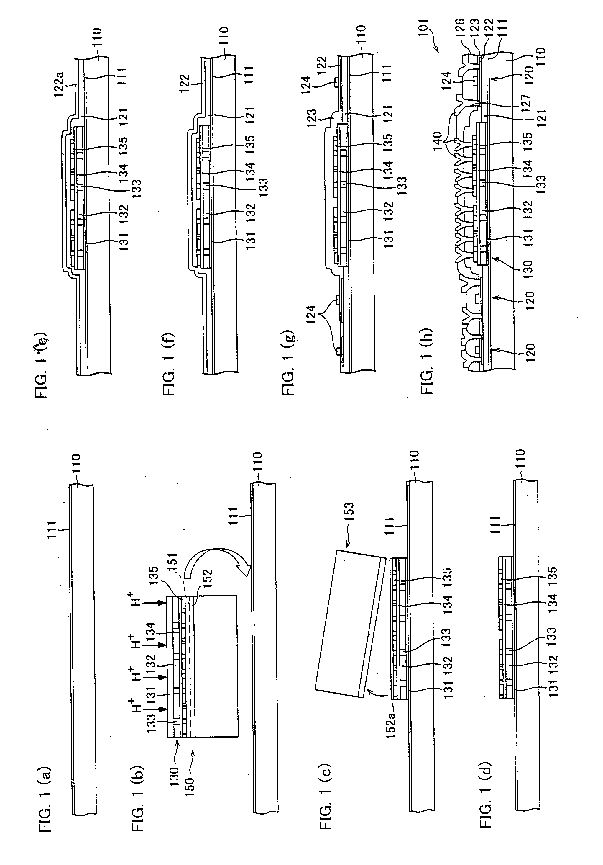
[0047] The following will describe an embodiment of a semiconductor device of the present invention and a method of manufacturing the same.

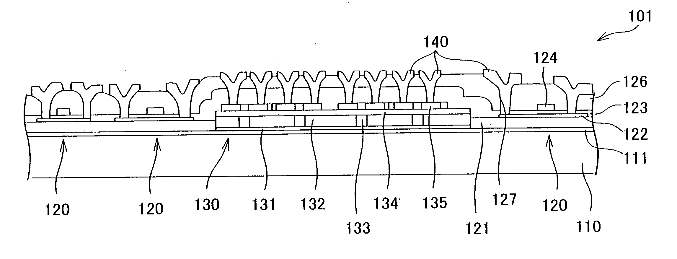
[0048] A semiconductor device 101 of the present embodiment is arranged in such a manner that a polycrystalline silicon thin-film transistor (non-single-crystal silicon thin-film transistor; non-single-crystal silicon thin-film device) 120 and a MOS (Metal Oxide Semiconductor) single-crystal silicon thin-film transistor (single-crystal silicon thin-film device) 130 are integrated on different regions on an insulating substrate. As FIG. 7 shows, the semiconductor device 101 can be further integrated, as a driving circuit 710, on an active matrix substrate 700 having a display section 720.

[0049] As illustrated in FIG. 8, the semiconductor device 101 is arranged so that, on an insulating substrate 110, an SiO2 (oxidized silicon) film (oxidized film) 111, the MOS polycrystalline silicon thin-film transistor 120 including a polycrystalline silicon t...

embodiment 2

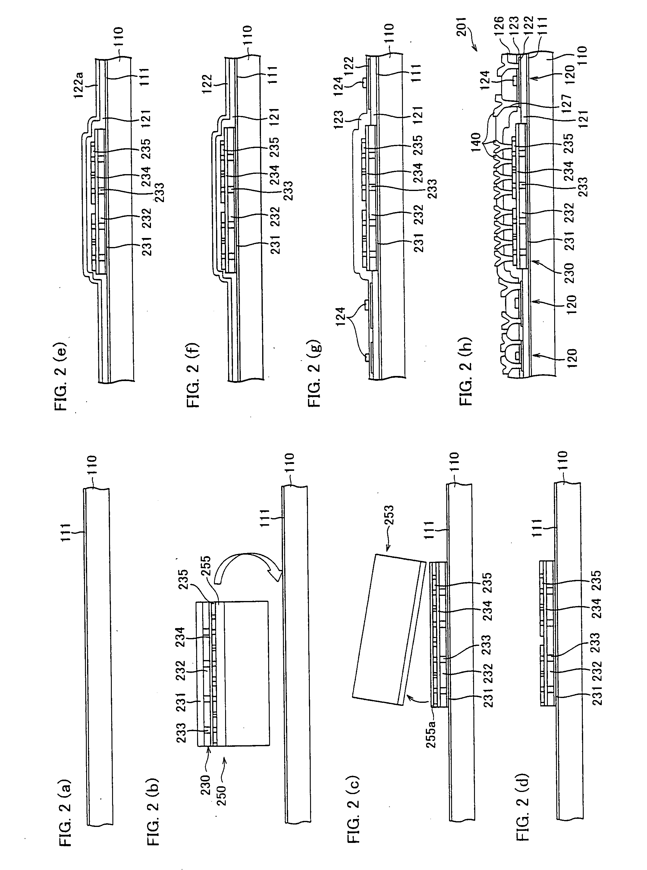
[0102] The following will discuss another embodiment of a semiconductor device of the present invention and a manufacturing method thereof, with reference to figures. By the way, members having the same functions as those described in the semiconductor device 101 of Embodiment 1 are given the same numbers, so that the descriptions are omitted for the sake of convenience.

[0103] Being similar to the semiconductor device 101 of Embodiment 1, a semiconductor device 201 of the present embodiment is arranged in such a manner that a polycrystalline silicon thin-film transistor 120 and a MOS single-crystal silicon thin-film transistor 230 are integrated in different regions on an insulating substrate, and the device 201 is utilized for, for instance, an active matrix substrate. For this reason, the semiconductor device 201 is arranged identical with the semiconductor device 101 of Embodiment 1.

[0104] However, the semiconductor device 201 is different from the semiconductor device 101 of E...

embodiment 3

[0144] The following will describe a further embodiment of a semiconductor device of the present invention and a method of manufacturing the same. By the way, members having the same functions as those described in the semiconductor device 101 of Embodiment 1 are given the same numbers, so that the descriptions are omitted for the sake of convenience.

[0145] As shown in FIG. 10, a semiconductor device 301 of the present embodiment is identical with the semiconductor device 101 of Embodiment 1 to the extent that a single-crystal silicon thin film device and a non-single-crystal silicon thin film device are formed in different regions on an insulating substrate.

[0146] Note that, however, the semiconductor device 301 is different from the semiconductor device 101 of Embodiment 1 to the extent that the non-single-crystal silicon thin film device is formed from a continuous grain silicon thin film 322. The continuous grain silicon is polycrystalline silicon formed in such a way that, by...


PUM


Abstract

On an SOI substrate, a hydrogen ion implantation section in which distribution of hydrogen ions peaks in a BOX layer (buried oxide film layer), and a single-crystal silicon thin-film transistor are formed. Then this SOI substrate is bonded with an insulating substrate. Subsequently, the SOI substrate is cleaved at the hydrogen ion implantation section by carrying out heat treatment, so that an unnecessary part of the SOI substrate is removed, Furthermore, the BOX layer remaining on the single-crystal silicon thin-film transistor is removed by etching. With this, it is possible to from a single-crystal silicon thin-film device on an insulating substrate, without using an adhesive. Moreover, it is possible to provide a semiconductor device which has no surface damage and includes a single-crystal silicon thin film which is thin and uniform in thickness.

Description

CROSS-REFERENCE TO RELATED APPLICATIONS [0001] This application is a divisional of application Ser. No. 10 / 802,735, filed Mar. 18, 2004, which claims priority under 35 U.S.C. § 119(a) to Patent Application No. 2003-077283 filed in Japan on Mar. 20, 2003. The entire contents of Application No. 2003-077283 are hereby incorporated by reference.FIELD OF THE INVENTION [0002] The present invention relates to SOI technology, and particularly relates to a semiconductor device utilized for a high-performance integrated circuit formed on a low-priced general-purpose insulating substrate and a TFT-driven active matrix LCD, OLED and the like. BACKGROUND OF THE INVENTION [0003] There have been so-called active matrix driving devices which drive, for instance, liquid crystal display panels and organic EL display panels and are constructed in such a manner that a thin-film transistor (TFT) made of amorphous silicon (amorphous Si; a-Si) or polycrystalline silicon (p-Si) is formed on a glass substra...

Claims


Application Information

Patent Timeline
Patent Type & Authority Applications(United States)
IPC IPC(8): H01L29/04H01L21/30H01L29/786H01L27/12H01L21/02H01L21/336H01L21/58H01L21/60H01L21/68H01L21/762H01L21/77
CPCH01L21/6835H01L2924/1305H01L21/76259H01L24/24H01L24/26H01L24/82H01L24/83H01L27/1214H01L27/1266H01L2221/68359H01L2221/68363H01L2224/24226H01L2224/8319H01L2224/8385H01L2224/83894H01L2924/01004H01L2924/01005H01L2924/01013H01L2924/01015H01L2924/01029H01L2924/0103H01L2924/01033H01L2924/01039H01L2924/01046H01L2924/0105H01L2924/01056H01L2924/01074H01L2924/01078H01L2924/01082H01L2924/04953H01L2924/07802H01L2924/09701H01L2924/14H01L2924/3025H01L2924/01006H01L2924/01019H01L2924/01021H01L2924/01023H01L2924/0132H01L21/76254H01L2924/1306H01L2924/13091H01L2924/12041H01L2924/01014H01L2924/01022H01L2924/3512H01L2924/00H01L2924/15788H01L2924/12042H01L2924/12044H01L27/1218
Inventor TAKAFUJI, YUTAKAITOGA, TAKASHI
Owner TAKAFUJI YUTAKA
Why Eureka
Try Eureka