Method of photoresist strip for plasma doping process of semiconductor manufacturing

a technology of semiconductor manufacturing and photoresist strip, which is applied in the direction of semiconductor devices, electrical equipment, basic electric elements, etc., can solve the problems of difficult removal of the photoresist layer from the substrate, downstream processing problems, and shallow source/drain junctions

Active Publication Date: 2007-10-18
MICRON TECH INC
View PDF19 Cites 26 Cited by
  • Summary
  • Abstract
  • Description
  • Claims
  • Application Information

AI Technical Summary

Benefits of technology

[0011] While the specification concludes with claims particularly pointing out and distinctly claiming that which is regarded as the present invention, the advantage

Problems solved by technology

During subsequent processing, the photoresist layer is difficult to remove from the substrate due to the presence of the dopant-containing layer and a carbon-rich crust on the photoresist layer.
Hydrogen fluoride is typically provided in a ratio with deionized water of 100:1 to 500:1 However, these solutions cause streaking defects across the substrate, which leads to downstream processing problems.
However, one difficulty with CMOS processing

Method used


Image

  • Method of photoresist strip for plasma doping process of semiconductor manufacturing
  • Method of photoresist strip for plasma doping process of semiconductor manufacturing
  • Method of photoresist strip for plasma doping process of semiconductor manufacturing

Examples


example 1

Water Rinse of Boron-Implanted Semiconductor Wafer

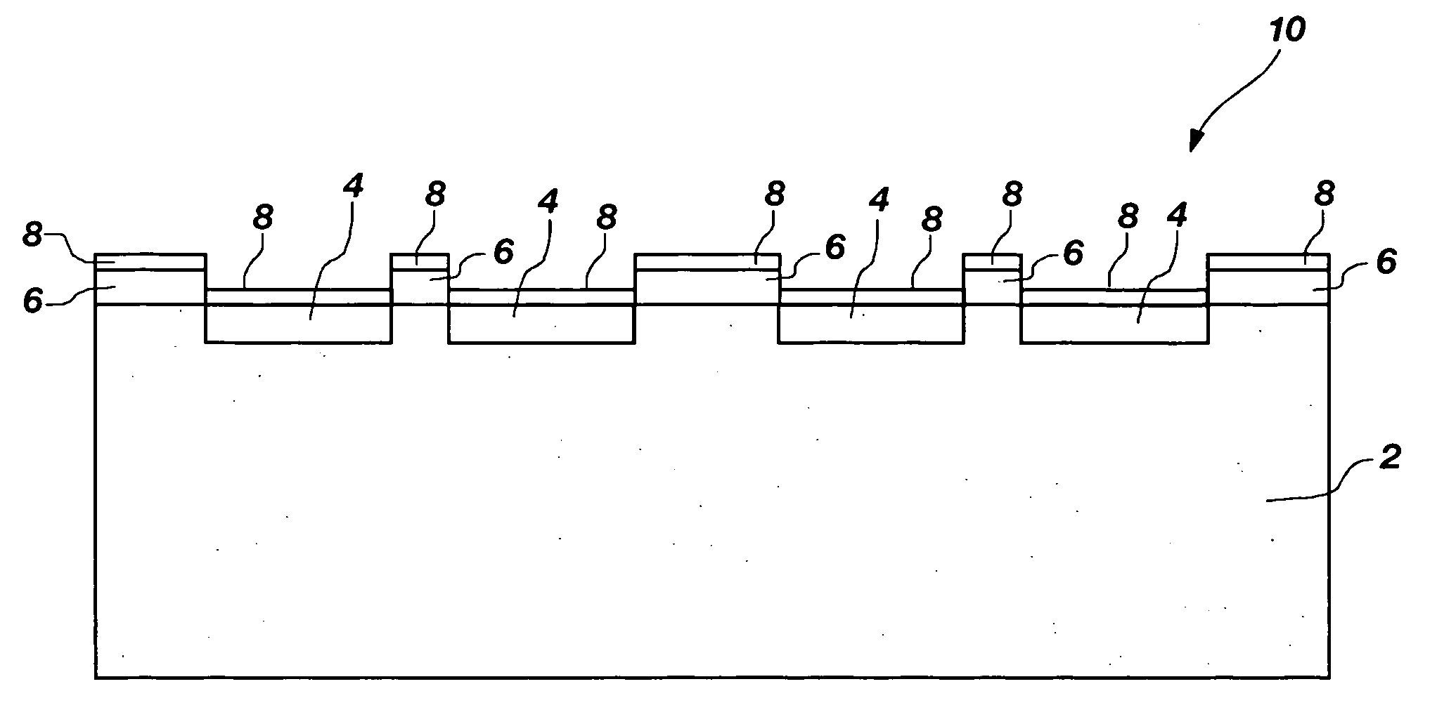
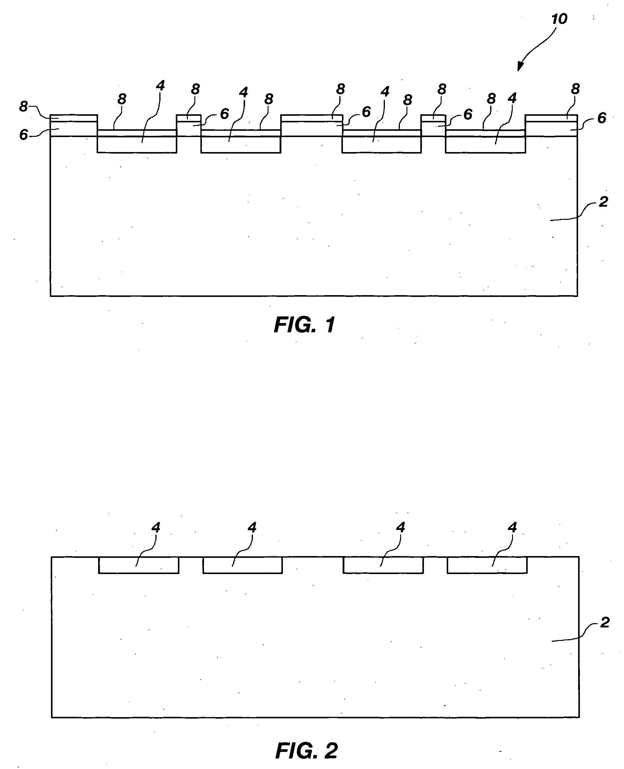
[0040] A semiconductor wafer was implanted with boron by PLAD using 15% B2H6 and 85% H2 at −6 kV, 60 μsec / 5 kHz pulse, a dose of 2×10¹⁶ / cm2 dose, a RF power of 725 W, and a pressure of 6 mTorr. The semiconductor wafer was implanted with the boron through a photoresist mask formed from a carbon-based photoresist material. Using SEPR-402, the photoresist pattern on the implanted semiconductor wafer is shown in FIG. 4. The implantation produced a boron-containing layer having approximately 70% boron and approximately 20% oxygen and a thickness of approximately 212 Å on the photoresist layer of the semiconductor wafer. The semiconductor wafer was exposed to a water rinse that included DI water maintained at a temperature that ranged from approximately 55° C. to approximately 65° C. The semiconductor wafer was exposed to the water rinse for approximately 5 minutes. The semiconductor wafer was then dried using conventional surface tension...

example 2

Fluorinated Plasma Treatment of Boron-Implanted Semiconductor Wafer

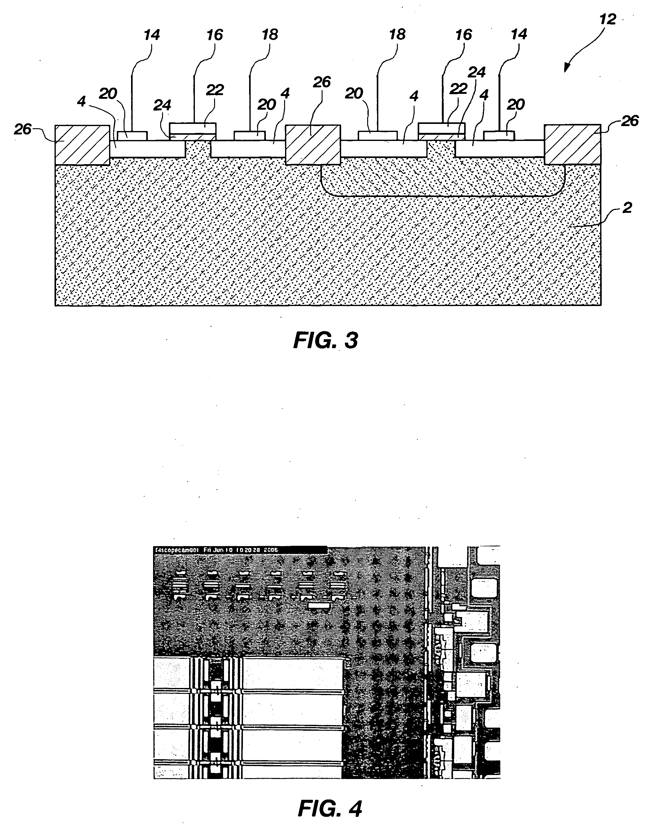
[0042] A semiconductor wafer was implanted with boron by PLAD using 15% B2H6 and 85% H2 at −6 kV, 60 μsec / 5 kHz pulse, a dose of 2×10¹⁶ / cm2, a RF power of 725 W, and a pressure of 6 mTorr. The semiconductor wafer was implanted with boron using a photoresist mask formed from a carbon-based (SEPR-402) photoresist material. The implantation produced a boron-containing layer having approximately 70% boron and approximately 20% oxygen and a thickness of approximately 212 Å on the photoresist layer of the semiconductor wafer. The semiconductor wafer was exposed to a CF4 plasma that also included O2 and a forming gas (3.6% H2 in N2). The CF4 was present at approximately 70 standard cubic centimeters per minute (“scm”), the O2 was present at approximately 2000 sccm, and the forming gas was present at approximately 1500 sccm. The CF4 plasma was generated at a power of approximately 1800 W, a temperature of approximately 180°...


PUM


Abstract

A method of forming an intermediate semiconductor device is disclosed that comprises providing a semiconductor substrate, forming a photoresist layer on the semiconductor substrate, implanting a dopant into the semiconductor substrate, and removing a dopant-containing layer from the photoresist layer. The dopant-containing layer includes dopant residuals and a carbon-rich crust and may be formed during implantation. The dopant-containing layer may be removed from the photoresist layer by exposing the dopant-containing layer to a water rinse, a chlorinated plasma or to a fluorinated plasma. The water rinse may include deionized water that is maintained at a temperature that ranges from approximately 25° C. to approximately 80° C. The fluorinated plasma may be formed from a gaseous precursor selected from the group consisting of nitrogen trifluoride, carbon tetrafluoride, trifluoromethane, hexafluoroethane, sulfur hexafluoride, and mixtures thereof. A method of forming an ultrashallow junction is also disclosed.

Description

FIELD OF THE INVENTION [0001] The present invention relates to a method of manufacturing an intermediate semiconductor device. More specifically, the present invention relates to a method of removing a photoresist layer from the intermediate semiconductor device, where the photoresist layer is covered by a dopant-containing layer. The dopant-containing layer is removed from the photoresist layer without affecting the photoresist layer or other exposed layers on the intermediate semiconductor device. BACKGROUND OF THE INVENTION [0002] To implant dopants in junctions of a semiconductor device, plasma doping (“PLAD”) (also know as plasma immersion ion implantation (“PIII”)) and beamline ion implantation have been used. Beamline ion implantation is a high energy implantation technique where ions penetrate deeply into a substrate, semiconductor wafer, or other workpiece. In contrast, PLAD has unique advantages including system simplicity, lower cost and higher throughput. [0003] In PLAD,...

Claims


Application Information

Patent Timeline
IPC IPC(8): H01L21/426
CPCH01L21/2236H01L29/78H01L21/31138H01L21/31133
Inventor QIN, SHUMCTEER, ALLENHANSON, ROBERT J.
Owner MICRON TECH INC
Why Eureka
Try Eureka