Optical semiconductor device having diffraction grating

a technology of optical semiconductor and diffraction grating, which is applied in the direction of lasers, laser optical resonator construction, laser details, etc., can solve the problems of increasing cost, reducing and increasing the cost of regrowth, so as to achieve the effect of increasing the resistance of the devi

Inactive Publication Date: 2007-10-25
FUJITSU LTD +1
View PDF4 Cites 30 Cited by
  • Summary
  • Abstract
  • Description
  • Claims
  • Application Information

AI Technical Summary

Benefits of technology

[0013] The narrow width portion suppresses the higher order transverse ...

Problems solved by technology

It is necessary for the regrowth method (1) to perform crystal growth twice, which is likely to increase cost.
If the surface of the lower growth layer is made of material ...

Method used


Image

  • Optical semiconductor device having diffraction grating
  • Optical semiconductor device having diffraction grating
  • Optical semiconductor device having diffraction grating

Examples


Embodiment Construction

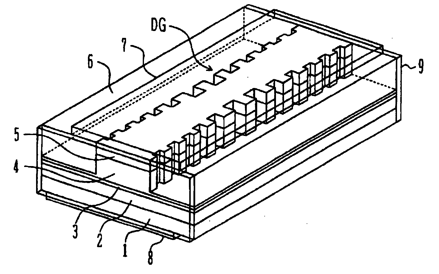
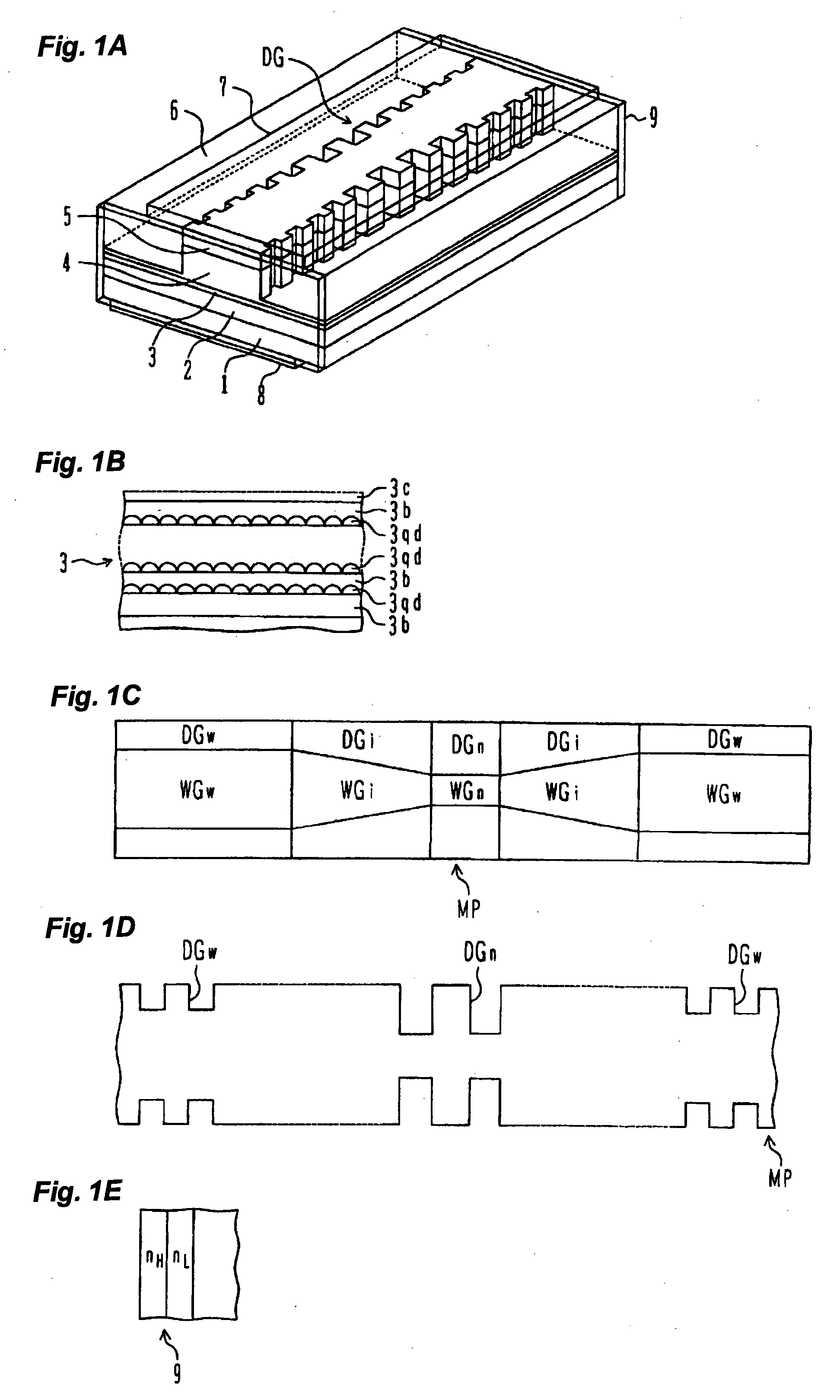
[0018]FIG. 1A shows a ridge type laser according to the first embodiment of the present invention. Formed on an n-type (001) GaAs substrate 1 by molecular beam epitaxy (MBE) are: an n-type Al0.4Ga0.6As clad layer 2 having a thickness of 1.4 μm; an active layer 3 including multiple quantum dot layers; a p-type Al0.4Ga0.6As clad layer 4 having a thickness of 1.4 μm; and a p-type GaAs contact layer 5 having a thickness of 0.4 μm.

[0019] As shown in FIG. 1B, the active layer 3 having ten quantum dot layers is formed by the following processes. After a GaAs barrier layer 3b having a thickness of, e.g., 36 nm is grown, InAs having a large lattice mismatch is grown in molecular layer order to form an InAs quantum dot layer 3qd by a self formation method in Stranski-Krastanov growth mode (S-K mode) which forms quantum dots at a thickness larger than a critical thickness. This InAs quantum dot layer is covered with a GaAs barrier layer 3b having a thickness of 36 nm. Further, pairs of simila...


PUM


Abstract

An optical semiconductor device includes: a waveguide structure including layers grown over a semiconductor substrate, having a width defined by sidewalls formed by etching the layers, and including a wide, a narrow, and an intermediate width portion, formed along a propagation direction; and a diffraction grating formed on the sidewalls of at least one of the wide and narrow width portions of the waveguide structure, the diffraction grating having vertical grooves periodically disposed along the propagation direction and defining a wavelength of propagation light, wherein the narrow width portion is formed in such a manner that a loss of 50% or more is given to a higher order transverse mode. An optical semiconductor device having a vertical diffraction grating is provided which can suppress generation of a higher order transverse mode and an increase in a device resistance.

Description

CROSS REFERENCE TO RELATED APPLICATION [0001] This application is based on and claims priority of Japanese Patent Application No. 2006-065791 filed on Mar. 10, 2006, the entire contents of which are incorporated herein by reference. BACKGROUND OF THE INVENTION [0002] A) Field of the Invention [0003] The present invention relates to an optical semiconductor device having a diffraction grating, and more particularly to an optical semiconductor device having a vertical groove diffraction grating. [0004] B) Description of the Related Art [0005] The following methods are known as a method of forming a diffraction grating of a distributed feedback (DFB) laser or a distributed Bragg reflector (DBR) laser: (1) a regrowth method by which a diffraction grating pattern is formed on the surface of a lower growth layer, and an upper crystal growth layer is regrown on the lower growth layer to form a diffraction grating at the interface of the growth layer; and (2) collective etching method by wh...

Claims


Application Information

Patent Timeline
IPC IPC(8): H01S5/12
CPCB82Y20/00H01S5/0655H01S5/1064H01S5/12H01S5/34306H01S5/1225H01S5/1237H01S5/22H01S5/3412H01S5/1212
Inventor HATORI, NOBUAKIYAMAMOTO, TSUYOSHIARAKAWA, YASUHIKO
Owner FUJITSU LTD
Why Eureka
Try Eureka