

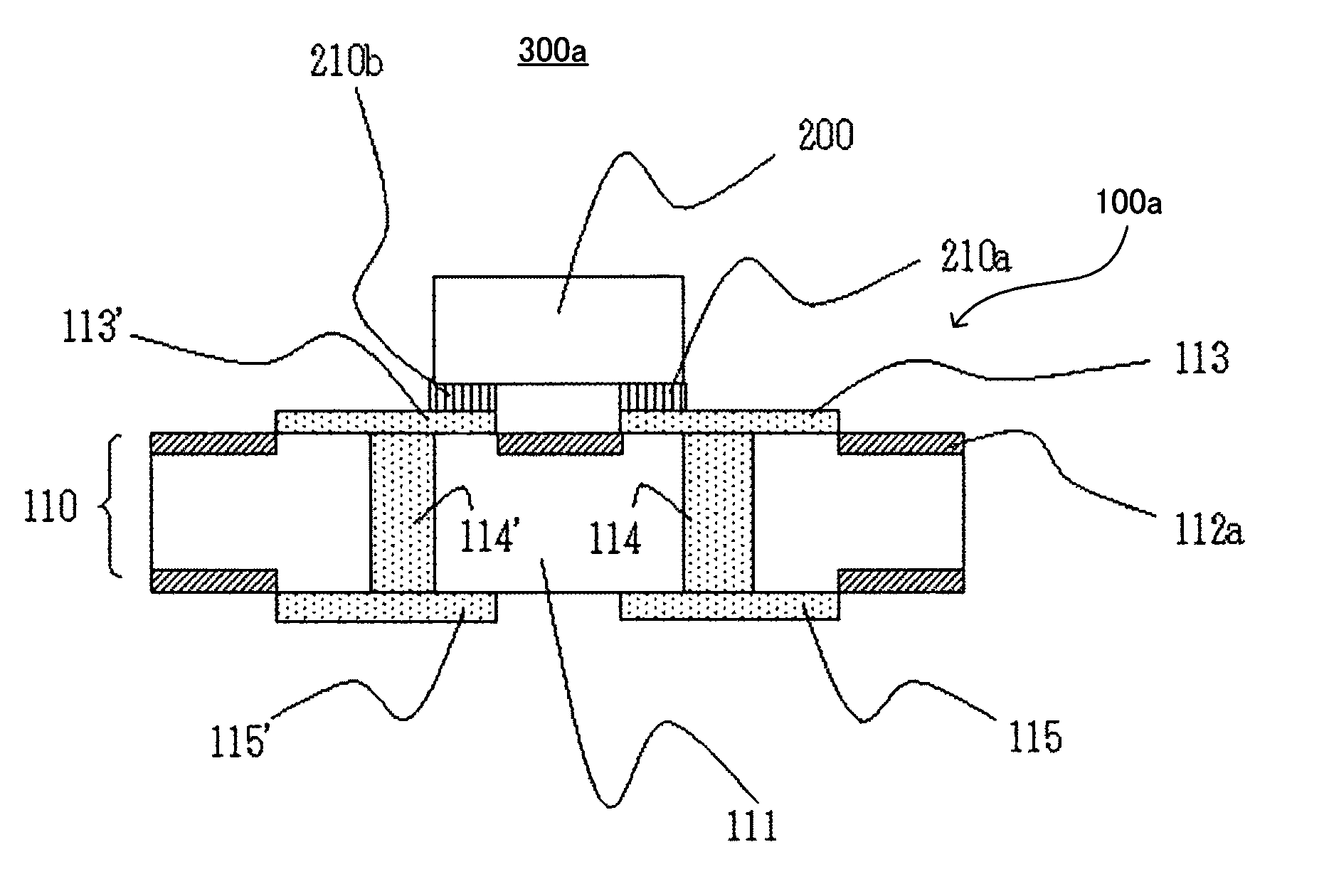
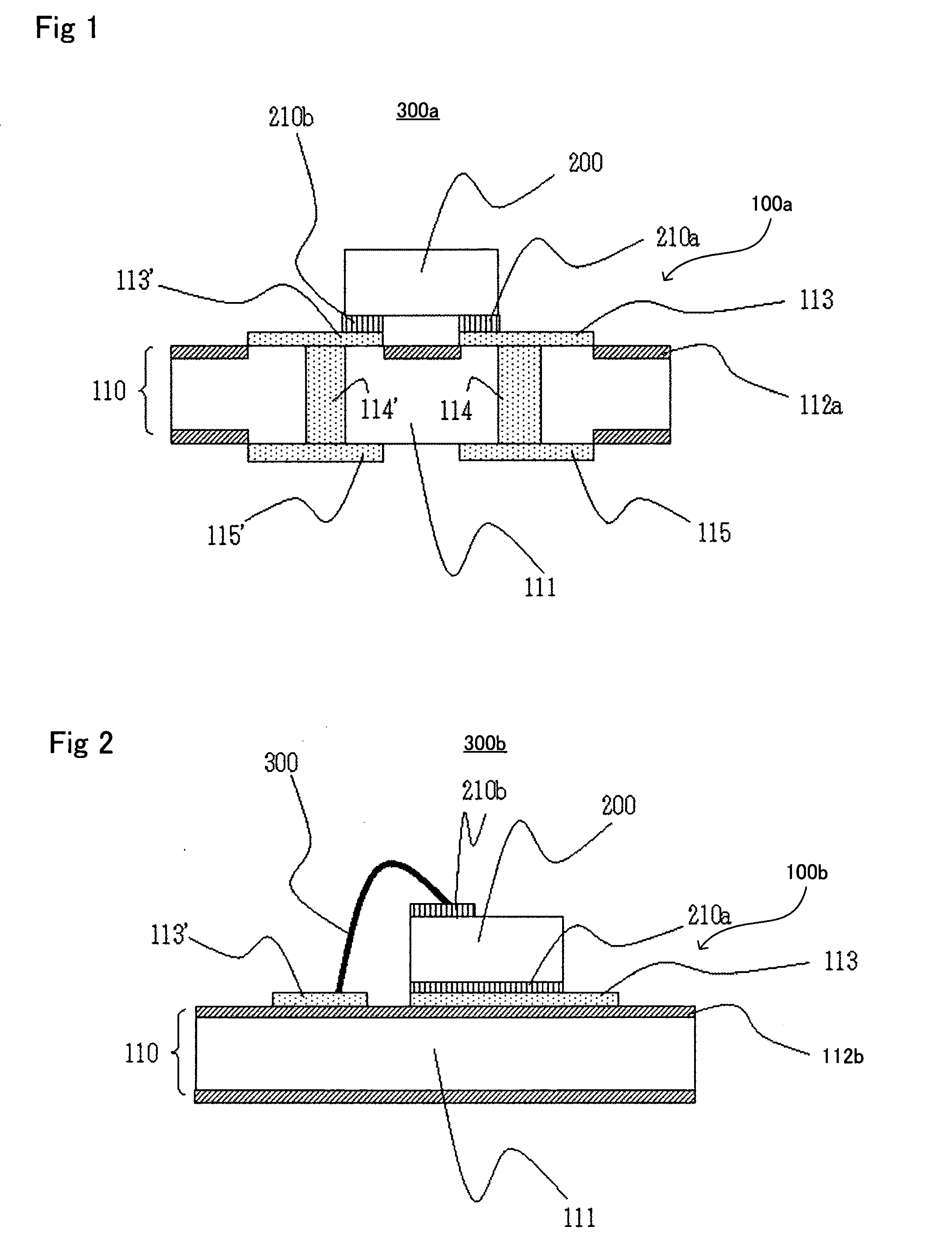
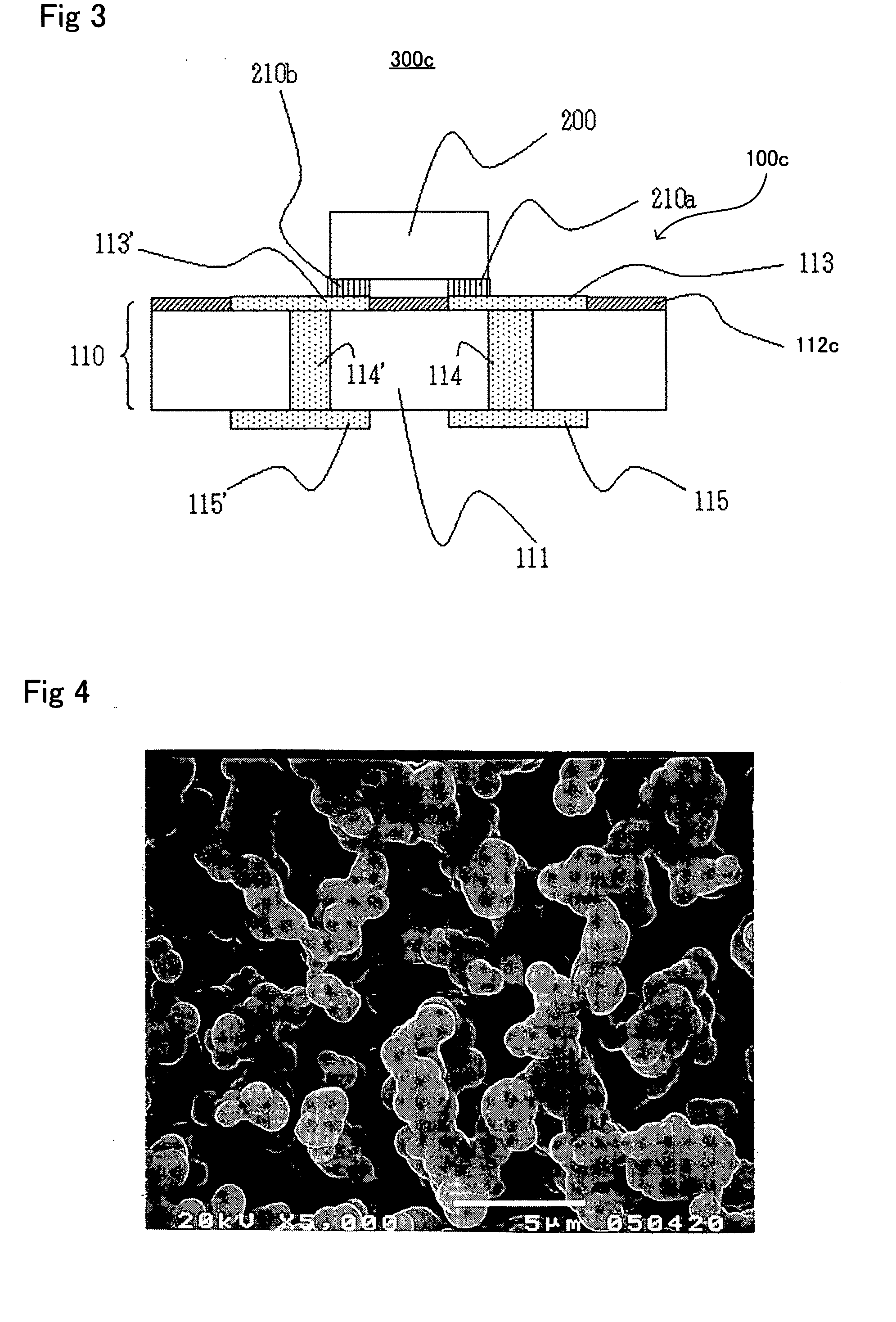
Ceramic Substrate for Mounting a Light Emitting Element and Method for Manufacturing the Same
a technology of light emitting elements and ceramic substrates, which is applied in the direction of discharge tubes/lamp details, discharge tubes/solid-state device details, and discharge tubes/lamp details, etc., can solve the problems of reducing the luminance of complex light emitting elements, exposing the possibility of damage to light emitting elements, and difficult to radiate heat from light emitting elements, etc., to achieve the effect of raising the luminance of the light emitting element and suppressing damag
- Summary
- Abstract
- Description
- Claims
- Application Information
AI Technical Summary
Benefits of technology
Problems solved by technology
Method used
Image

Examples
example 1
An Example Having Used an Aluminum Nitride Substrate on a Surface of Which a Coat Layer Constituted of Oxide Imparting a Surface a High Light Reflectance was Formed by Being Subjected to Sufficient Oxidation Treatment
[0076] Mixed in a ball mill were 100 parts by mass of aluminum nitride powder, 5.0 parts by mass of yttrium oxide, 1.0 part by mass of tetraglycerine monoolate, as a surfactant; 40 parts by mass of toluene as a solvent, 13 parts by mass of poly n-butyl methacrylate as a binder, 4.2 parts by mass of dibutyl phthalate as a plasticizer, 10 parts by mass of toluene, 5 parts by mass of butyl acetate to obtain a white slurry. Then, the obtained slurry was subjected to forming into the shape of a sheet by means of a doctor blade to prepare an insulating substrate green sheet with a thickness of 0.6 mm. The obtained green sheet was heated for degreasing at 850° C. for 2 hr in a flow of hydrogen gas containing water at 10 litters / min. Note that a temperature rise rate in degrea...
example 2
An Example Using an Aluminum Nitride Substrate on a Surface of Which a Coat Layer Constituted of a White Ceramics is Coated.
[0079] A white ceramic paste was prepared by mixing 68 parts by mass of boron nitride powder, 9 parts by mass of boron oxide powder, 23 parts by mass of aluminum nitride powder, 26 parts by mass of ethyl cellulose and 110 parts by mass of terpineol as a solvent. Then, the obtained paste was coated on one surface of an aluminum nitride green sheet adjusted in a similar way to that in Example 1 by means of a printing method to form a paste layer with a thickness of 15 μm. Thereafter, degreasing and firing were conducted in a similar way to that in Example 1 to form the coat layer (with a thickness of 10 μm) constituted of boron nitride. Note that a tone of a surface of the coat layer was of a white color. The obtained sintered body was evaluated on a reflectance for light having wave length of from 300 to 800 nm on the surface of the coat layer, a density and a ...
example 3
An Example Using an Aluminum Nitride Substrate on a Surface of Which a Coat Layer Constituted of a White Ceramics (Boron Nitride) is Coated)
[0080] A white ceramic paste was prepared in a similar way to that in Example 2 with the exception that a composition of a white ceramic paste that was used was such that 68 parts by mass of boron nitride powder, 23 parts by mass of aluminum nitride powder, 18 parts by mass of yttrium oxide, 28 parts by mass of ethyl cellulose and 120 parts by mass of terpineol (solvent), then the obtained paste was coated on a an aluminum nitride green sheet, and degreased and sintered in a similar way to that in Example 2. The obtained sintered body substrate had the coat layer (with a thickness of 10 μm) constituted of boron nitride and a tone of the coated layer was white. The obtained sintered body was evaluated on a reflectance for light having wavelength of from 300 to 800 nm on the surface of the coated layer, density and thermal conductivity in a simil...
PUM
| Property | Measurement | Unit |
|---|---|---|
| optical reflectance | aaaaa | aaaaa |
| optical reflectance | aaaaa | aaaaa |
| thickness | aaaaa | aaaaa |
Abstract
Description
Claims
Application Information