Manufacturing method of semiconductor device

a manufacturing method and semiconductor technology, applied in the direction of single crystal growth, polycrystalline material growth, chemistry apparatus and processes, etc., can solve the problems of high substrate cost, high substrate cost, and high manufacturing cost of lsis made using soi substrates, and achieve low cost, high film thickness controllability, and high crystal quality.

Active Publication Date: 2007-11-22
RENESAS ELECTRONICS CORP
View PDF4 Cites 14 Cited by
  • Summary
  • Abstract
  • Description
  • Claims
  • Application Information

AI Technical Summary

Benefits of technology

[0024] To solve the foregoing problems, the inventors have tried a variety of approaches concerning the manufacture of the SOI structure by the ELO method. As a result, the inventors have found that an epitaxial growth surface is planarized as shown in FIGS. 4A and 4B through the step of etching and flattening of the epitaxial growth surface in an HCl or hydrogen gas ambience, carried out consecutively following growth of a single-crystal Si layer through selective epitaxial growth. It has been found that the etching and flattening process consecutively performed on the epitaxial growth surface without allowing, even once, the temperature of the substrate, increased during growth, to cool down to room temperature makes a facet formed during the epitaxial growth disappear. It has further been found that letting the substrate temperature cool down to the room temperature after the substrate surface has been planarized allows the aforementioned effect of stress arising from the facet shape to be suppressed, making it possible to form the SOI structure having no stacking faults as shown in an enclosure 70 in FIGS. 4A and 4B. The present invention has been completed based on the foregoing findings.
[0025] According to the foregoing aspects of the present invention, the SOI structure can be formed on the bulk substrate. The SOI substrate can therefore be provided at low cost. The substrate surface is planarized through the hydrogen annealing offering high film thickness controllability without using the CMP method. The SOI layer offering a high crystal quality free from crystal defects can therefore be formed uniformly. As a result, SOI substrates can be manufactured at low cost and with high yield. In addition, according to the aspects of the present invention, the SOI region and the bulk region can coexist on a single substrate. This allows the high blocking voltage devices and ESD protective devices for preventing ESD (electrostatic discharge) breakdown to be formed as a bulk type MISFET on the same substrate. This helps reduce a region occupied by substrates, as compared with an arrangement in which the SOI type MISFET, which offers the outstanding characteristics of low power consumption and high speed, and the bulk type MISFET are formed on respective substrates and then connected together to each other. Moreover, the processes for manufacturing the SOI type MISFET and the bulk type MISFET are used in common, which realizes the manufacture of both wafers without making the processes complicated.

Problems solved by technology

The SOI substrate used for making the SOI type MISFET is generally extremely expensive as compared with a bulk substrate used conventionally.
In either type, the manufacturing process is complicated, resulting in a high substrate cost.
There is therefore a problem that LSIs made using the SOI substrates require a high manufacturing cost as compared with those made using bulk substrates.
The very use of the CMP in this technique leads to an increased cost.
Disadvantageously, the foregoing technique using the CMP has problems in controllability and uniformity of the film thickness and thus finds it difficult to achieve the aforementioned design rule.
In addition to the uniformity problem, the conventional ELO method entails a problem of defects that occur in the manufactured SOI structure. FIGS. 3A and 3B are views showing a cross section of an SOI structure manufactured through the conventional ELO.
From the foregoing discussion, it is difficult to suppress stacking faults and manufacture a SOI structure offering a high crystal quality as long as the conventional ELO method is used and surface flattening is performed using the CMP.
The MISFET manufactured on the SOI substrate generally develops degradation of source-drain blocking voltage, thus limiting its application only to a low voltage region.
It has been difficult to form high blocking voltage devices or ESD protective devices for preventing ESD (electrostatic discharge) breakdown on the SOI substrate.
The region occupied by the substrates then cannot be made small, which eventually results in inability to making the entire semiconductor device small.
This poses a problem of complicating the processes.

Method used


Image

  • Manufacturing method of semiconductor device
  • Manufacturing method of semiconductor device
  • Manufacturing method of semiconductor device

Examples


first embodiment

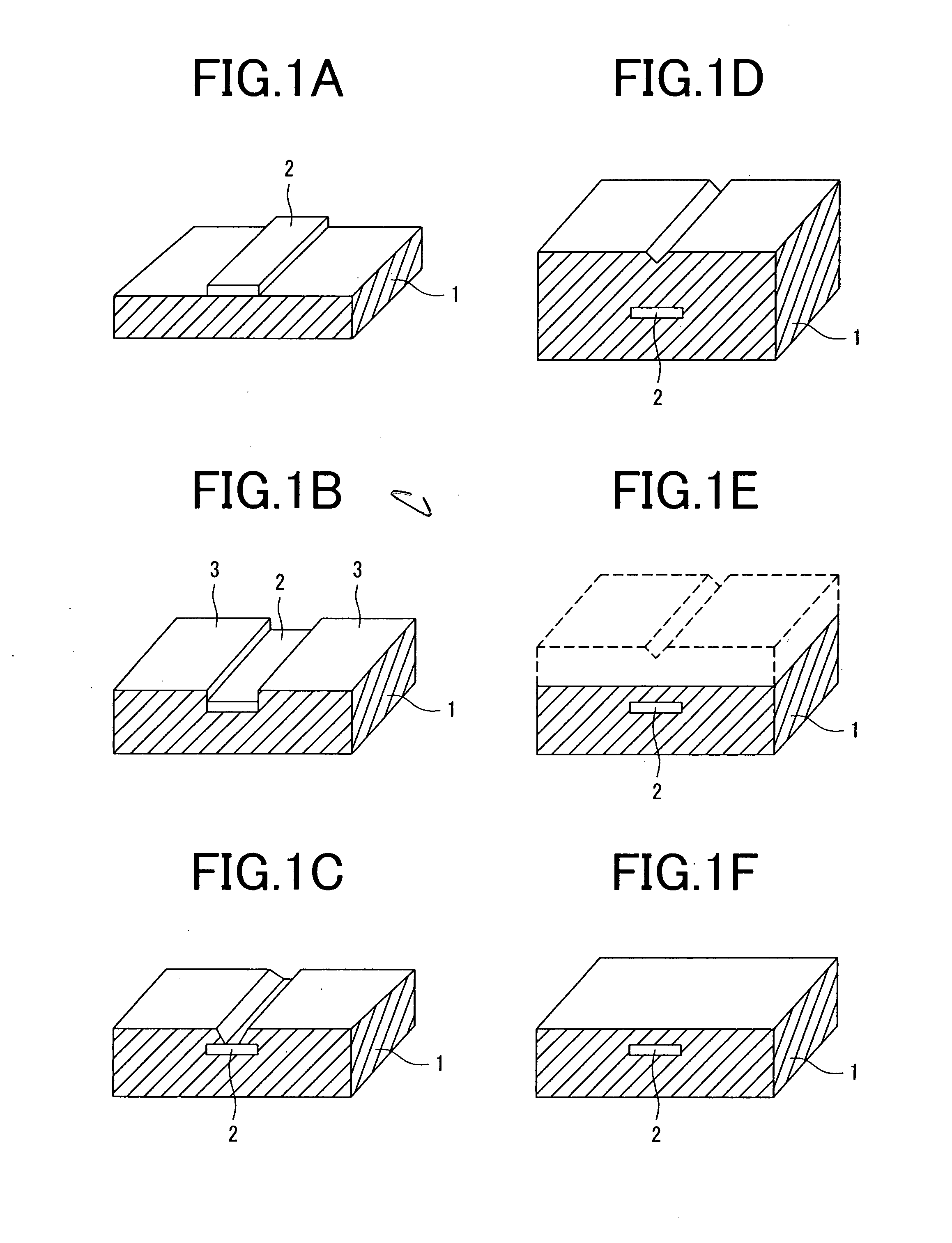
[0050]FIGS. 1A through 1F are views illustrating steps for manufacturing an SOI structure according to a first embodiment of the present invention. For the sake of convenience, the conductivity type of semiconductor substrates and semiconductor films is fixed; however, specific conductivity types may be combined in any arbitrary ways and are not limited to those described in the embodiments.

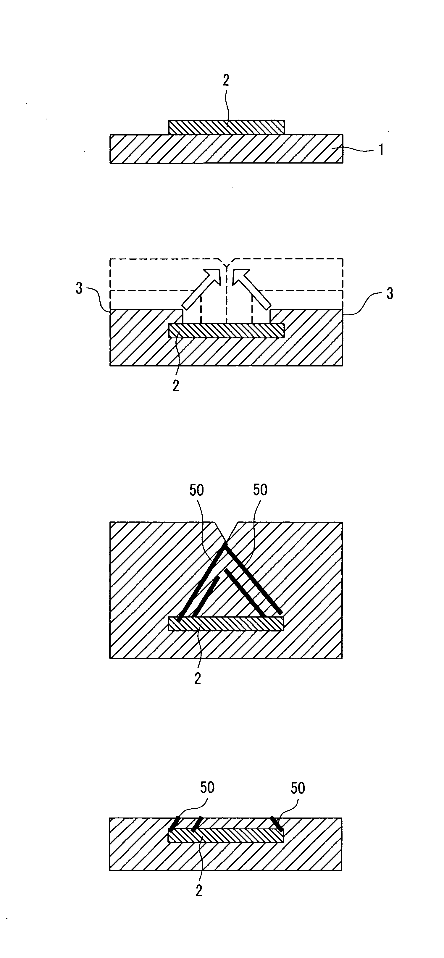
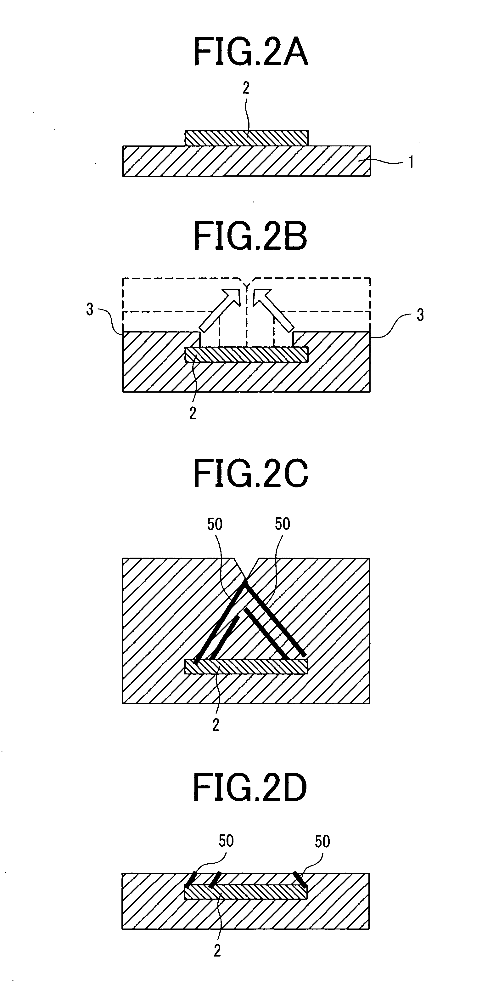
[0051] A silicon oxide film 2 having a thickness, for example, of 10 nm is formed as an embedded oxide film layer on a semiconductor substrate 1 including a 20-cm-diameter single-crystal Si having a plain orientation (100), P-type conductivity, and a resistivity of 10 ohm.cm and having a main surface subjected to mirror polishing. Photoresist is subsequently applied and the silicon oxide film on a region on which the SOI structure is not to be formed is selectively removed (FIG. 1A). Selective epitaxial growth of Si is then performed in two stages. It is commonly known that, in the selective epi...

second embodiment

[0053] A semiconductor device according to a second embodiment of the present invention will be described below with reference to FIGS. 5A through 5G. A silicon oxide film 2 having a thickness, for example, of 10 nm is formed as an embedded oxide film layer (FIG. 5A) on a semiconductor substrate 1 including a 20-cm-diameter single-crystal Si having a plain orientation (100), P-type conductivity, and a resistivity of 10 ohm.cm and having a main surface subjected to mirror polishing. Photoresist is subsequently applied and the silicon oxide film on a region on which the SOI structure is not to be formed is selectively removed (FIG. 5B). Selective epitaxial growth of Si is then performed at a relatively low temperature region. It is commonly known that, in the selective epitaxial growth of Si, introducing the HCl gas during the growth process enhances selectivity on Si and the oxide film.

[0054] The introduction of the HCl gas, however, promotes etching of the silicon oxide film also. ...

third embodiment

[0057] A semiconductor device according to a third embodiment of the present invention will be described below with reference to FIGS. 6A through 6D. Photoresist is applied to a semiconductor substrate 1 including a 20-cm-diameter single-crystal Si having a plain orientation (100), P-type conductivity, and a resistivity of 10 ohm.cm and having a main surface subjected to mirror polishing. The single-crystal Si is then selectively etched (FIG. 6A). A silicon oxide film 4 is subsequently formed to form an embedded oxide film layer. At this time, controlling the film thickness of the silicon oxide film 4 allows the embedded oxide film layer with a desired film thickness to be formed. Thereafter, hydrogen annealing at a high temperature of, for example, 1050° C., is performed to etch Si. As noted earlier, etching progresses from a peripheral portion for a patterned silicon oxide film. By making use of this characteristic, it is possible to etch the silicon oxide film only on edge portio...


PUM

PropertyMeasurementUnit
thicknessaaaaaaaaaa
threshold voltageaaaaaaaaaa

Abstract

It is an object of the present invention to provide a method of manufacturing an SOI wafer at low cost and with high yield. It is another object of the present invention to provide a semiconductor device including also bulk type MISFETs used as high voltage regions and a method of manufacturing the same without using complicated processes and increasing the size of a semiconductor chip. The method of manufacturing a semiconductor device comprises selectively epitaxially growing a single-crystal Si layer and continuously performing the epitaxial growth without bringing a substrate temperature increased during the growth to room temperature even once. An epitaxially grown surface is then etched and planarized. The substrate temperature is then cooled down to the room temperature.

Description

CLAIM OF PRIORITY [0001] The present application claims priority from Japanese Application JP 2006-139944, filed on May 19, 2006, the content of which is hereby incorporated by reference into this application. BACKGROUND OF THE INVENTION [0002] 1. Field of the Invention [0003] The present invention relates generally to methods of manufacturing MISFETs having a stacked structure of a semiconductor, an insulator, and a metal and, more particularly, to a method of manufacturing a semiconductor device including a MISFET formed on a semiconductor substrate having an SOI (Silicon-on-Insulator) structure. [0004] 2. Description of the Related Arts [0005] With the greater integration and greater performance achieved lately in LSI technology, further miniaturization of MISFETs (metal-insulator-semiconductor field effect transistors) has been progressed. As a result, gate length is scaled to make more conspicuous the problem of a short channel effect that involves a reduced threshold voltage V...

Claims


Application Information

Patent Timeline
Patent Type & Authority Applications(United States)
IPC IPC(8): C30B23/00C30B25/00C30B28/12C30B28/14
CPCC30B25/00C30B23/00
Inventor TSUCHIYA, RYUTAKIMURA, YOSHINOBUMORITA, YUSUKE
Owner RENESAS ELECTRONICS CORP
Why Eureka
Try Eureka