

Laser processing of workpieces containing low-k dielectric material
a dielectric material and workpiece technology, applied in the field of laser machining, can solve the problems of reducing the service life of the dicing blade,
- Summary
- Abstract
- Description
- Claims
- Application Information
AI Technical Summary
Benefits of technology
Problems solved by technology
Method used
Image

Examples
Embodiment Construction
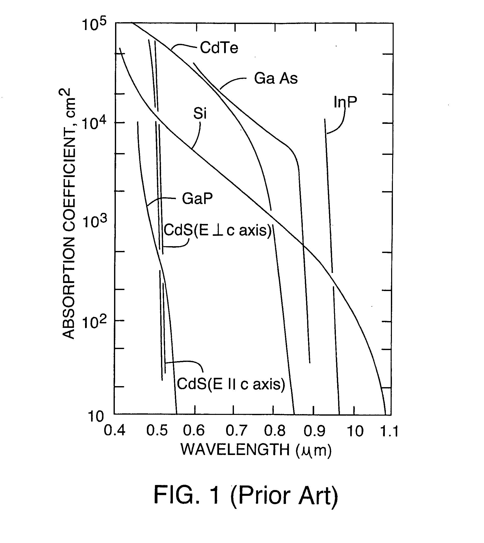
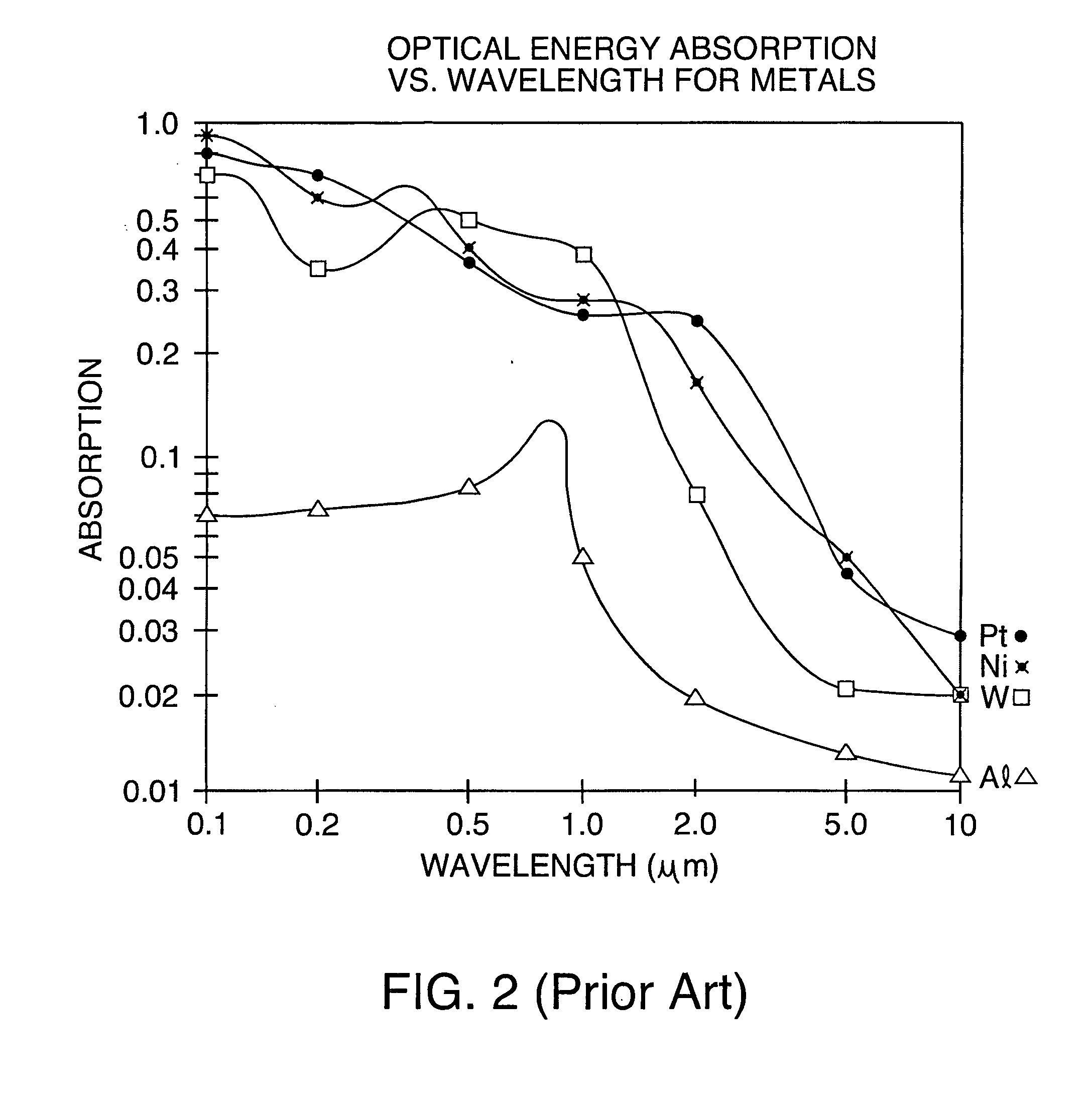
[0024]Although laser processing capability has advanced greatly in the last few years due to advances both in available lasers and in process understanding, there are still some significant issues with the use of lasers for dicing, drilling, or patterning processes. Attempts may have been made to use infrared (IR) lasers to machine silicon or silicon oxides. Some traditional IR wavelengths have, to a limited extent, been shown to machine these materials and have been used successfully as laser scribing tools for marking die or for limited scribe-and-break applications. These lasers, however, tend to damage silicon by, for example, unpredictably cracking the silicon or oxide layers; throwing permanent redeposited material, such as melted slag, onto the top surface of the wafer; and creating a “melt lip” where the edge of the kerf pulls backward and up.
[0025]U.S. Pat. Nos. 5,593,606 and 5,841,099 ('099 patent) of Owen et al. describe techniques and advantages for employing ultraviolet...
PUM
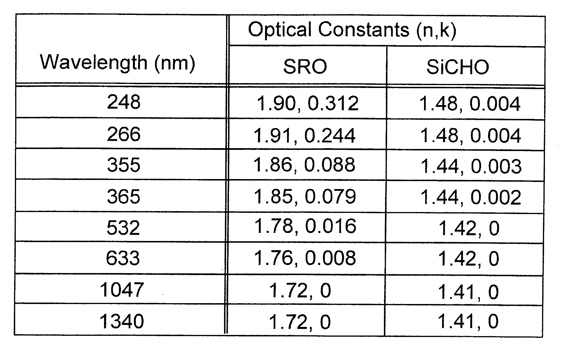
| Property | Measurement | Unit |
|---|---|---|
| wavelength | aaaaa | aaaaa |
| wavelength | aaaaa | aaaaa |
| wavelength | aaaaa | aaaaa |
Abstract
Description
Claims
Application Information