Chemical mechanical polishing pad

a technology of mechanical polishing and polishing pads, applied in the field of polishing pads, can solve the problems of increasing the cost of cmp consumables, and increasing the cost of manufacturing tools,

Active Publication Date: 2007-11-29
ROHM & HAAS ELECTRONICS MATERIALS CMP HLDG INC
View PDF15 Cites 21 Cited by
  • Summary
  • Abstract
  • Description
  • Claims
  • Application Information

AI Technical Summary

Problems solved by technology

The fabrication of these semiconductor devices continues to become more complex due to requirements for devices with higher operating speeds, lower leakage currents and reduced power consumption.
The devices' smaller scale and increased complexity have led to greater demands on CMP consumables, such as polishing pads and polishing solutions.
In addition, as integrated circuits' feature sizes decrease, CMP-induced defectivity, such as, scratching becomes a gre...

Method used


Image

  • Chemical mechanical polishing pad
  • Chemical mechanical polishing pad
  • Chemical mechanical polishing pad

Examples


example 1

[0034]The polymeric pad materials were prepared by mixing various amounts of isocyanates as urethane prepolymers with 4,4′-methylene-bis-o-chloroaniline [MBCA] at 50° C. for the prepolymer and 116° C. for MBCA. In particular, various toluene diiosocyanate [TDI] with polytetramethylene ether glycol [PTMEG] prepolymers provided polishing pads with different properties. The urethane / polyfunctional amine mixture was mixed with the hollow polymeric microspheres (EXPANCEL® 551DE20d60 or 551DE40d42 manufactured by AkzoNobel) either before or after mixing the prepolymer with the chain extender. The microspheres had a weight average diameter of 15 to 50 μm, with a range of 5 to 200 μm, and were blended at approximately 3,600 rpm using a high shear mixer to evenly distribute the microspheres in the mixture. The final mixture was transferred to a mold and permitted to gel for about 15 minutes.

[0035]The mold was then placed in a curing oven and cured with a cycle as follows: thirty minutes ramp...

example 2

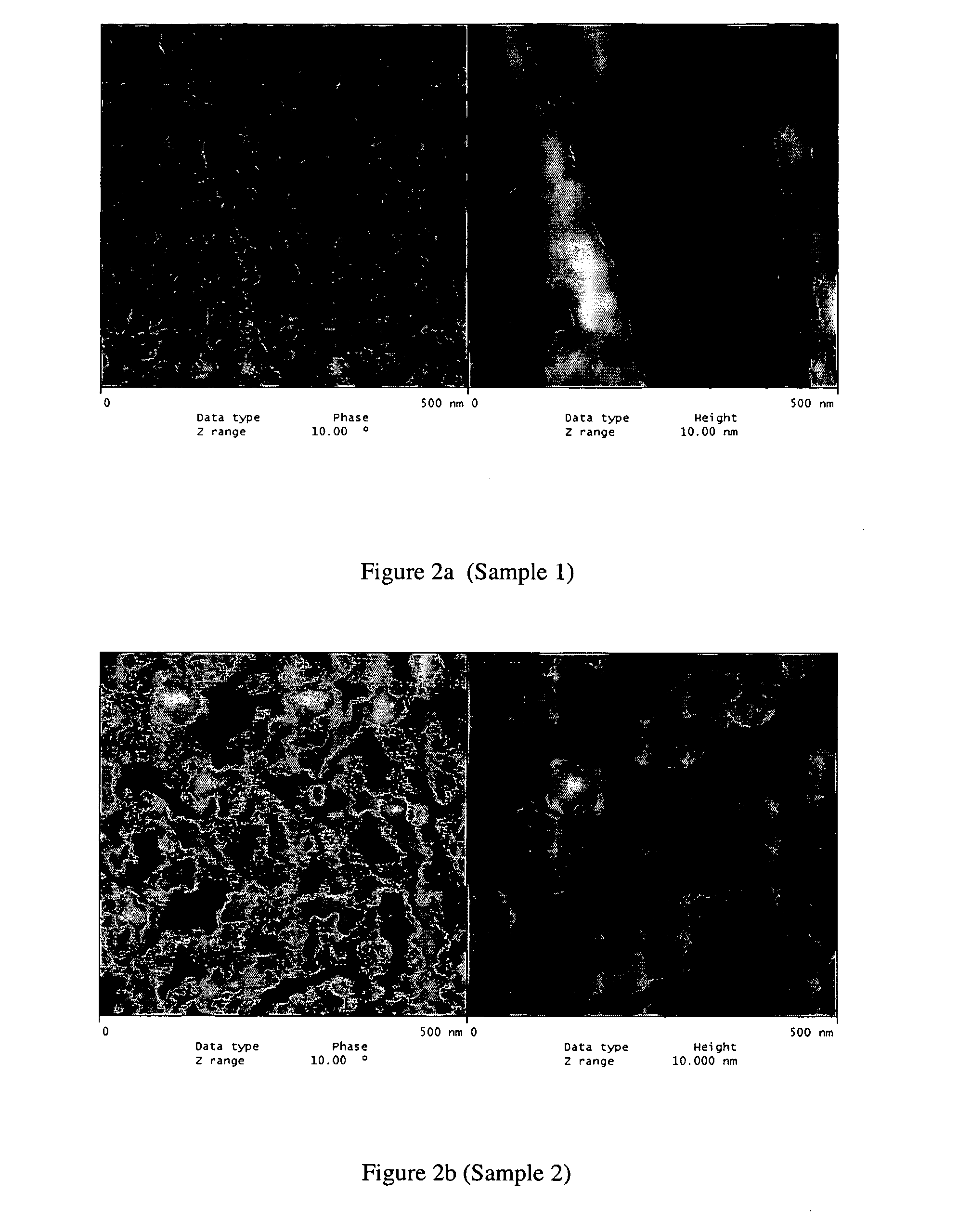
[0041]FIGS. 2A to 2D illustrate four samples of polyurethane imaged using SPM techniques. These techniques were modified to amplify the differences in different regions of the samples based on their hardness, allowing the hard and soft phases to be imaged. To carry out the experiment an FESP tip with a low spring constant was used to give additional sensitivity. All sampling parameters were kept constant during the experiment for all samples analyzed. A setpoint ratio of 0.8 was chosen to collect the images. The two images for each sample show the sample phase distribution on the left and the corresponding topography for that same region on the right.

[0042]FIGS. 2A and 2B (Samples 1 and 2) correspond to polyurethanes having distinct two phase structure of hard phase and soft phase, with ratio of purest hard phase to purest soft phasec (Sample B) lacks a distinct two-phase structure. FIG. 2d (Sample H) lacks sufficient purest soft phase relative to the amount of purest hard phase nec...

example 3

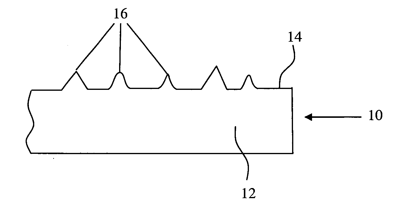
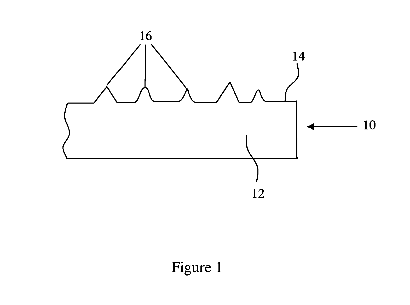
[0050]Pads of 80 mil (2.0 mm) thickness and 22.5 inch (57 cm) diameter were cut from cakes prepared with the process of Example 1. The pads included a circular groove pattern of 20 mil (0.51 mm) width, 30 mil (0.76 mm) depth and 70 mil (1.8 mm) pitch with an SP2150 polyurethane subpad. Polishing with a SpeedFam-IPEC 472 tool on platen 1 at 5 psi (34.5 KPa), 75 rpm platen speed and 50 rpm carrier speed provided comparative polishing data for the different pads. The polishing also relied upon a Kinik CG181060 diamond conditioner. The test wafers include TEOS sheet wafers, silicon nitride sheet wafers and 1 HDP MIT pattern wafer for measuring planarization of Celexis™ CX2000A ceria-containing slurry from Rohm and Haas Electronic Materials CMP Technologies.

TABLE 6Pore Level,Pore LevelAdded vol.,FormulationPoreg / 100 gcc / 100 gDensity,Shore DDesignationStoichiometrySizeformulationformulationg / ccHardness*B-185small3.21540.69750.4B-385small1.07180.95261.8B-385medium0.75180.96760.3B-185medium...


PUM

PropertyMeasurementUnit
Pore sizeaaaaaaaaaa
Percent by massaaaaaaaaaa
Pressureaaaaaaaaaa

Abstract

The invention provides a polishing pad suitable for planarizing at least one of semiconductor, optical and magnetic substrates. The polishing pad includes a polymeric matrix having a top polishing surface. The top polishing surface has polymeric polishing asperities or forms polymeric polishing asperities upon conditioning with an abrasive. The polymeric polishing asperities are from a polymeric material having at least 45 weight percent hard segment and a bulk ultimate tensile strength of at least 6,500 psi (44.8 MPa). And the polymeric matrix has a two phase structure, a hard phase and a soft phase with an average area of the hard phase to average area of the soft phase ratio of less than 1.6.

Description

BACKGROUND[0001]This specification relates to polishing pads useful for polishing and planarizing substrates, such as semiconductor substrates or magnetic disks.[0002]Polymeric polishing pads, such as polyurethane, polyamide, polybutadiene and polyolefin polishing pads represent commercially available materials for substrate planarization in the rapidly evolving electronics industry. Electronics industry substrates requiring planarization include silicon wafers, patterned wafers, flat panel displays and magnetic storage disks. In addition to planarization, it is essential that the polishing pad not introduce excessive numbers of defects, such as scratches or other wafer non-uniformities. Furthermore, the continued advancement of the electronics industry is placing greater demands on the planarization and defectivity capabilities of polishing pads.[0003]For example, the production of semiconductors typically involves several chemical mechanical planarization (CMP) processes. In each ...

Claims


Application Information

Patent Timeline
IPC IPC(8): B32B9/04B32B27/20B32B3/26
CPCB24D3/28B24B37/24Y10T428/249953Y10T428/31504Y10T428/31551H01L21/304
Inventor KULP, MARY JO
Owner ROHM & HAAS ELECTRONICS MATERIALS CMP HLDG INC
Why Eureka
Try Eureka