

Field-Effect Transistor, Semiconductor Device, a Method for Manufacturing Them, and a Method of Semiconductor Crystal Growth
a technology of field-effect transistors and semiconductor devices, which is applied in the direction of chemical vapor deposition coatings, radiation controlled devices, coatings, etc., can solve the problems that the surface of the uppermost semiconductor layer may not be formed, it is difficult to form the electrode on that rugged surface, and the electric characteristics such as connection strength and ohmic characteristics cannot become sufficiently stable, etc. achieve excellent crystallinity of the barrier layer, maintain the effect of composition speed and excellent flatness and smoothness
- Summary
- Abstract
- Description
- Claims
- Application Information
AI Technical Summary
Benefits of technology
Problems solved by technology
Method used
Image

Examples
embodiment 1
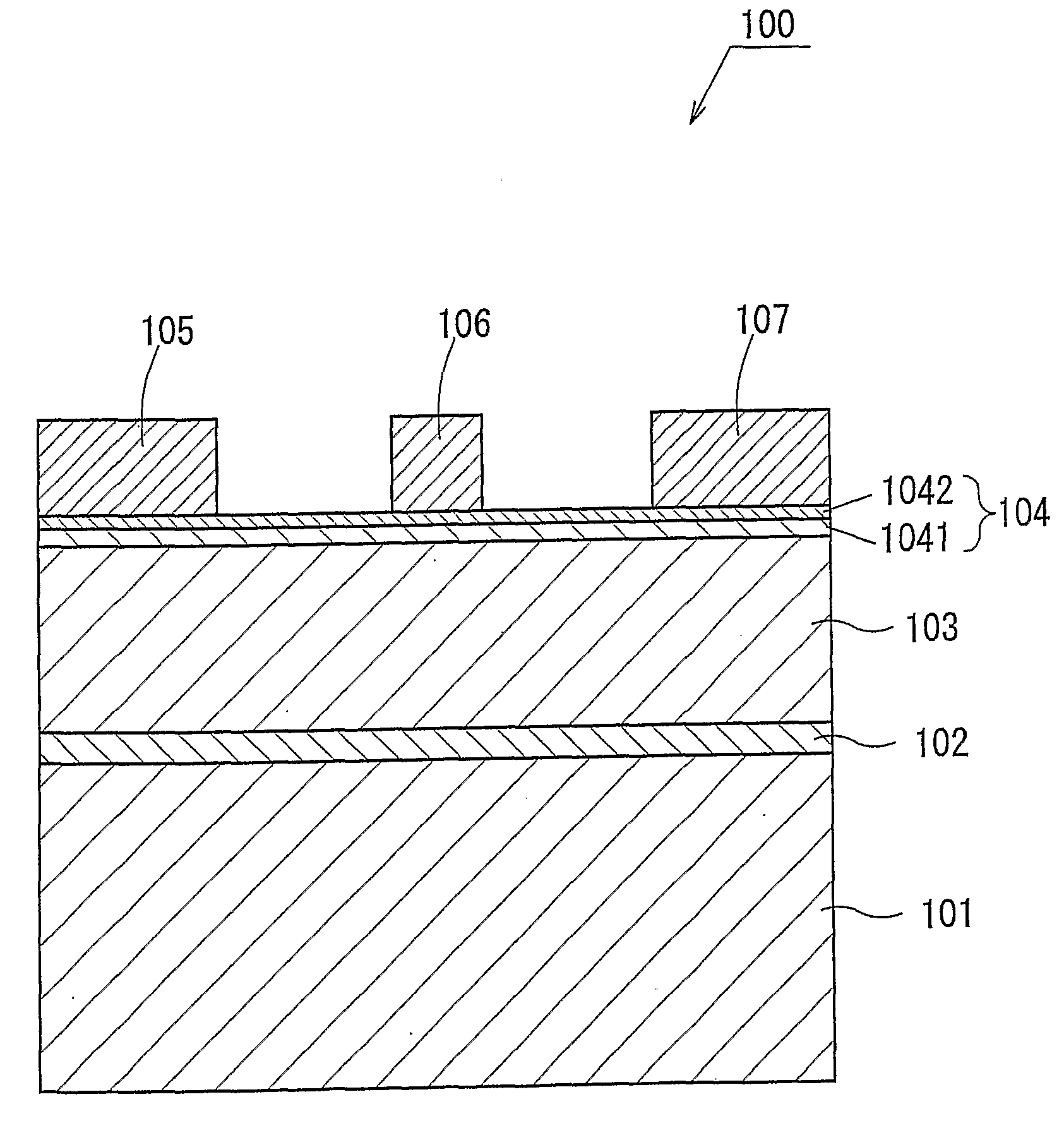
[0190]FIG. 1 is a sectional view of a field-effect transistor 100 in the first embodiment. The field-effect transistor 100 is a semiconductor device which is formed by depositing Group III nitride compound semiconductor layers in sequence through crystal growth, and a crystal growth substrate 101 is made of sapphire having thickness of about 300 μm. On the crystal growth substrate 101, about 40 nm in thickness of AlN layer 102 made of AlN is formed. The AlN layer 102 relaxes mismatch of lattice constants between the crystal growth substrate 101 and a semiconductor layer 103 formed on the AlN layer 102.
[0191] On the AlN layer 102, about 2 μm thickness of undoped GaN semiconductor layer 103 is formed. The semiconductor layer 103 and the AlN layer 102 are generically called a buffer layer hereinafter. The buffer layer (including the layer 102 and the layer 103) is a semiconductor layer referred to as a buffer layer in claims.
[0192] Further, on the semiconductor layer 103, about 40 nm...
embodiment 2
[0212]FIG. 5 is a sectional view of a field-effect transistor 200 of the second embodiment of the present invention. The field-effect transistor 200 is a semiconductor device which is formed by depositing Group III nitride compound semiconductors in sequence through crystal growth. A crystal growth substrate 201 is made of about 400 μm in thickness of silicon carbide (SiC). On the crystal growth substrate 201, about 0.2 μm in thickness of AlN layer 202 is formed. The AlN layer 202 removes or relaxes mismatch of lattice constants between the crystal growth substrate 201 and a semiconductor layer 203 formed on the AlN layer 202.
[0213] On the AlN layer 202, about 2 μm in thickness of undoped GaN semiconductor layer 203 is formed. The semiconductor layer 203 and the AlN layer 202 are generically called a buffer layer hereinafter. The buffer layer (including the layer 202 and the layer 203) is a semiconductor layer referred to as a buffer layer in claims.
[0214] Further, on the semicond...
modified embodiment 2
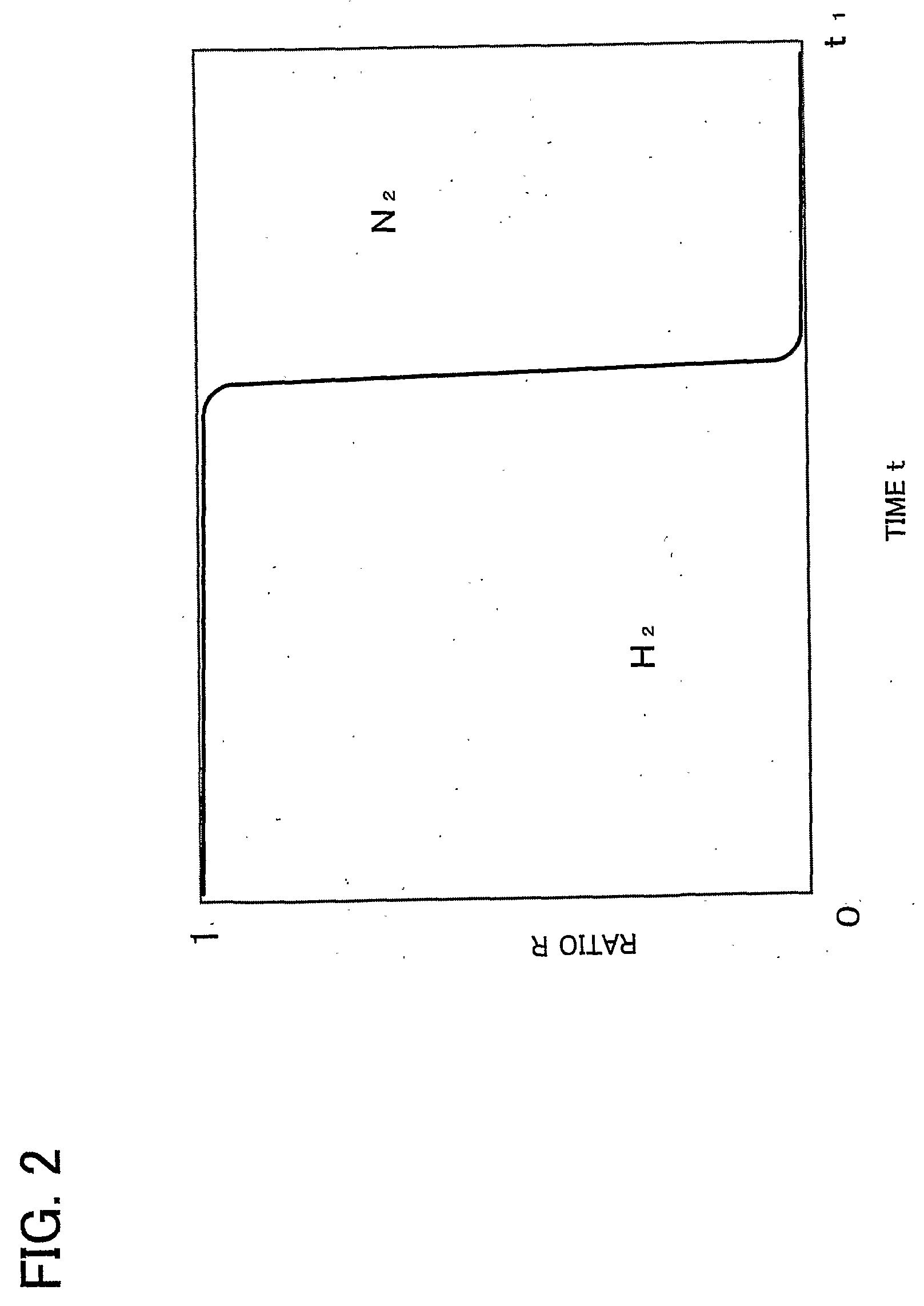
[0235] Alternatively, partial pressure ratio R of hydrogen gas in the carrier gas may be decreased gradually and momentarily. Further alternatively, decreasing process of the partial pressure ratio R can be a combination of smooth and consecutive decrease and rapid and step decrease. The embodiment as shown in FIG. 9 may includes such a combination of each decreasing process.
[0236] By employing any of these conditions, actions and effects of the present invention can be obtained according to the method of the present invention.
2. Explanation of the Eleventh to Twenty-Third Aspects
[0237] As a material which forms the crystal growth substrate comprised in the field-effect transistor of the present invention, silicon carbide (SiC) may be the most preferable considering thermal tightness and thermal radiation. Alternatively, sapphire, silicon (Si), or GaN can be used to form the substrate.
[0238] The ohmic electrode and the Schottky electrode can be formed by a well-known and arbitr...
PUM
| Property | Measurement | Unit |
|---|---|---|
| crystal growth temperature TA | aaaaa | aaaaa |
| crystal growth temperature TB | aaaaa | aaaaa |
| thickness | aaaaa | aaaaa |
Abstract
Description
Claims
Application Information