Nitride Semiconductor Device And Production Method Thereof

Inactive Publication Date: 2007-12-20
PANASONIC INTELLECTUAL PROPERTY MANAGEMENT CO LTD
View PDF13 Cites 100 Cited by
  • Summary
  • Abstract
  • Description
  • Claims
  • Application Information

AI Technical Summary

Benefits of technology

[0032] In a preferred embodiment, the second p-type nitride semiconductor layer fun

Problems solved by technology

Therefore, large strain is imposed on the active layer 106, so that the uniformity and reproducibility during the fabrication of the laser device are not very good.
However, although this method provides an improved steepness, Mg doping lags still occur in the AlGaN layers (which have a large band gap) so that non-uniformity of Mg concentration exists in the AlGaN layers.
Moreover, by forming a multitude of hetero interfaces, excesses and insufficiencies of Mg concentration irregularly occur within the crystal, thus resulting in a very low controllability and reproducibility.
However, in these conventional growing methods, although the Mg concentration has a constant value in the p-Al0.16Ga0.84 N electron over

Method used


Image

  • Nitride Semiconductor Device And Production Method Thereof
  • Nitride Semiconductor Device And Production Method Thereof
  • Nitride Semiconductor Device And Production Method Thereof

Examples


embodiment 1

[0065] Firstly, a first embodiment of the nitride semiconductor device according to the present invention will be described.

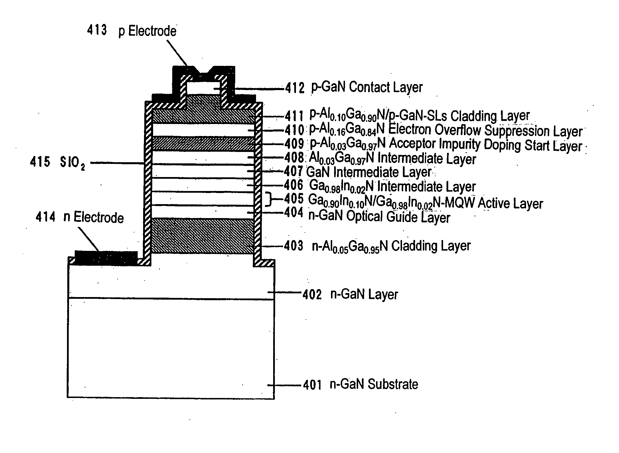
[0066]FIG. 4(a) shows a cross-sectional structure of the semiconductor laser of the present embodiment; and FIG. 4(b) is a schematic diagram of a conduction-band structure thereof. The semiconductor laser of the present embodiment includes an n-GaN substrate 401 and a semiconductor multilayer structure which is formed on the n-GaN substrate 401. Beginning from the substrate, this semiconductor multilayer structure includes: an n-GaN layer 402; an n-Al0.05Ga0.95N cladding layer 403; an n-GaN optical guide layer 404; a Ga0.90In0.10N / Ga0.98In0.02N-MQW active layer 405; a non-doped Ga0.98In0.02N intermediate layer 406; a non-doped GaN intermediate layer 407; a non-doped Al0.03Ga0.97N intermediate layer 408; a p-Al0.03Ga0.97N acceptor impurity doping start layer 409; a p-Al0.16Ga0.84N electron overflow suppression layer 410; a p-Al0.10Ga0.90N (2 nm thick) / p-GaN (2 ...

embodiment 2

[0117] In the present embodiment, after a semiconductor multilayer structure is formed similarly to Embodiment 1, this multilayer structure is processed into a stripe shape through a dry etching process. At this time, from the surface side, the p-GaN contact layer 412, the p-Al0.10Ga0.90N / p-GaN-SLs cladding layer 411, the p-Al0.16Ga0.84N electron overflow suppression layer 410, and the p-Al0.03Ga0.97N acceptor impurity doping start layer 409 are sequentially etched, almost until the non-doped Al0.03Ga0.97N intermediate layer 408 is exposed. The etching depth is an important parameter that determines the laser kink level and beam shape, and it is desirable to finely control the etching depth.

[0118] Monitor windows for optical evaluation, each being 50 μm per side, were provided in several places on the laser structure epitaxial wafer, and optical evaluations were performed in situ while conducting a dry etching process; thus, a dry etching was carried out.

[0119] In the present embo...

embodiment 3

[0122] Crystal growth for a laser structure was performed by using a construction similar to that of Embodiment 1, except for the structure of the p-type cladding layer. While Embodiment 1 employed the p-Al0.10Ga0.90N / p-GaN-SLs cladding layer 411, herein a p-Al0.08Ga0.92N / p-Al0.02Ga0.98N-SLs cladding layer 601 is used instead. FIG. 7(a) shows a structural diagram of this laser structure.

[0123] In the case where the p-Al0.10Ga0.90N / p-GaN-SLs cladding layer 411 is employed, supply / non-supply of TMA is periodically repeated to form AlGaN layers and GaN layers. If a uniform Mg doping is performed, the amount of Mg take-in will be reduced during the formation of the GaN layers, due to the memory effect. Conversely, when the AlGaN layers are formed, the amount of Mg take-in will rapidly increase near the interface. This will result in repetitive changes, each time stabilized at a constant value. Thus, as shown in FIG. 7(b), the Mg concentration is not stabilized within the cladding layer...


PUM


Abstract

A nitride semiconductor device according to the present invention includes a p-type nitride semiconductor layer, an n-type nitride semiconductor layer, and an active layer interposed between the p-type nitride semiconductor layer and the n-type nitride semiconductor layer. The p-type nitride semiconductor layer includes: a first p-type nitride semiconductor layer containing Al and Mg; and a second p-type nitride semiconductor layer containing Mg. The first p-type nitride semiconductor layer is located between the active layer and the second p-type nitride semiconductor layer, and the second p-type nitride semiconductor layer has a greater band gap than a band gap of the first p-type nitride semiconductor layer.

Description

TECHNICAL FIELD [0001] The present invention relates to nitride semiconductor devices. In particular, the present invention relates to: nitride semiconductor devices including semiconductor light-emitting devices, whose applications to photoelectronic information processing devices and illuminating light sources are considered promising, as well as bipolar-type transistors; and a production method thereof. BACKGROUND ART [0002] III-V group nitride semiconductors which contain nitrogen (N) as their V group element are regarded as promising materials for short-wavelength light-emitting devices, due to their large band gaps. Among others, vigorous researches are being directed toward gallium nitride-type compound semiconductors (GaN-type semiconductors: AlGaInN), and blue light-emitting diodes (LEDs) and green LEDs have already been put to practical use. Moreover, for the sake of realizing large-capacity optical disk apparatuses, semiconductor lasers having an oscillation wavelength in...

Claims


Application Information

Patent Timeline
IPC IPC(8): H01L29/06H01L21/20B82Y20/00H01L21/205H01S5/20H01S5/22H01S5/30H01S5/32H01S5/323H01S5/343
CPCB82Y20/00H01L33/04H01L33/32H01S5/2009H01S5/22H01S5/2214H01S5/3054H01S5/3063H01S5/3072H01S5/3077H01S5/3213H01S5/3216H01S5/34333H01S2304/04H01S5/3215H01L33/025H01L33/14
Inventor KAWAGUCHI, YASUTOSHISHIMAMOTO, TOSHITAKAISHIBASHI, AKIHIKOKIDOGUCHI, ISAOYOKOGAWA, TOSHIYA
Owner PANASONIC INTELLECTUAL PROPERTY MANAGEMENT CO LTD
Why Eureka
Try Eureka