Integrated Circuit, Method of Operating an Integrated Circuit, Method of Manufacturing an Integrated Circuit, Memory Module, Stackable Memory Module

a technology of integrated circuits and memory modules, applied in the direction of differential amplifiers, dc-amplifiers with dc-coupled stages, amplifiers, etc., can solve the problems of unnecessarily long circuit delays, rapid determination of the logic state of a memory device, and long waits, so as to increase the performance and speed of reading information stored in a memory device, actively balanced capacitive loads

Inactive Publication Date: 2008-01-03
POLARIS INNOVATIONS
View PDF26 Cites 157 Cited by
  • Summary
  • Abstract
  • Description
  • Claims
  • Application Information

AI Technical Summary

Benefits of technology

[0027] Embodiments of the present invention achieve technical advantages as a current sense amplifier and memory device having a current mirror with actively bala

Problems solved by technology

With unequal internal time constants, brief transient voltages and induced circuit noise may corrupt the resistance measurement process, requiring a longer wait time for reliable memory cell (e.g. MRAM cell) state determination.
A limiting factor often preventing the rapid determination of the logic state of a memory device is disparate time constants associated with parallel signal paths coupled to a voltage comparator in the memory cell state sensing circuit.
This produces a need for unnecessarily long circuit delays before the state of the voltage co

Method used


Image

  • Integrated Circuit, Method of Operating an Integrated Circuit, Method of Manufacturing an Integrated Circuit, Memory Module, Stackable Memory Module
  • Integrated Circuit, Method of Operating an Integrated Circuit, Method of Manufacturing an Integrated Circuit, Memory Module, Stackable Memory Module
  • Integrated Circuit, Method of Operating an Integrated Circuit, Method of Manufacturing an Integrated Circuit, Memory Module, Stackable Memory Module

Examples


Embodiment Construction

[0046] The making and using of exemplary embodiments are discussed in detail below. It should be appreciated, however, that the present invention provides many applicable inventive concepts that can be embodied in a wide variety of specific contexts. The specific embodiments discussed are merely illustrative of specific ways to make and use the invention, and do not limit the scope of the invention.

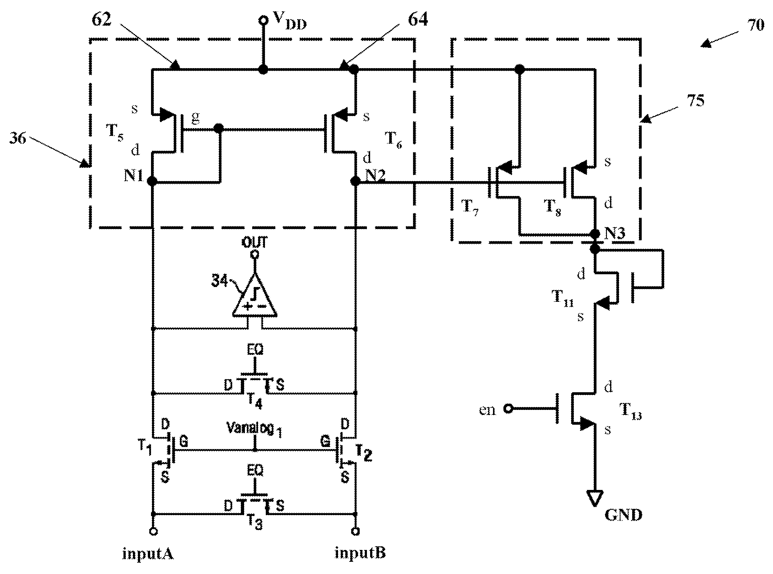
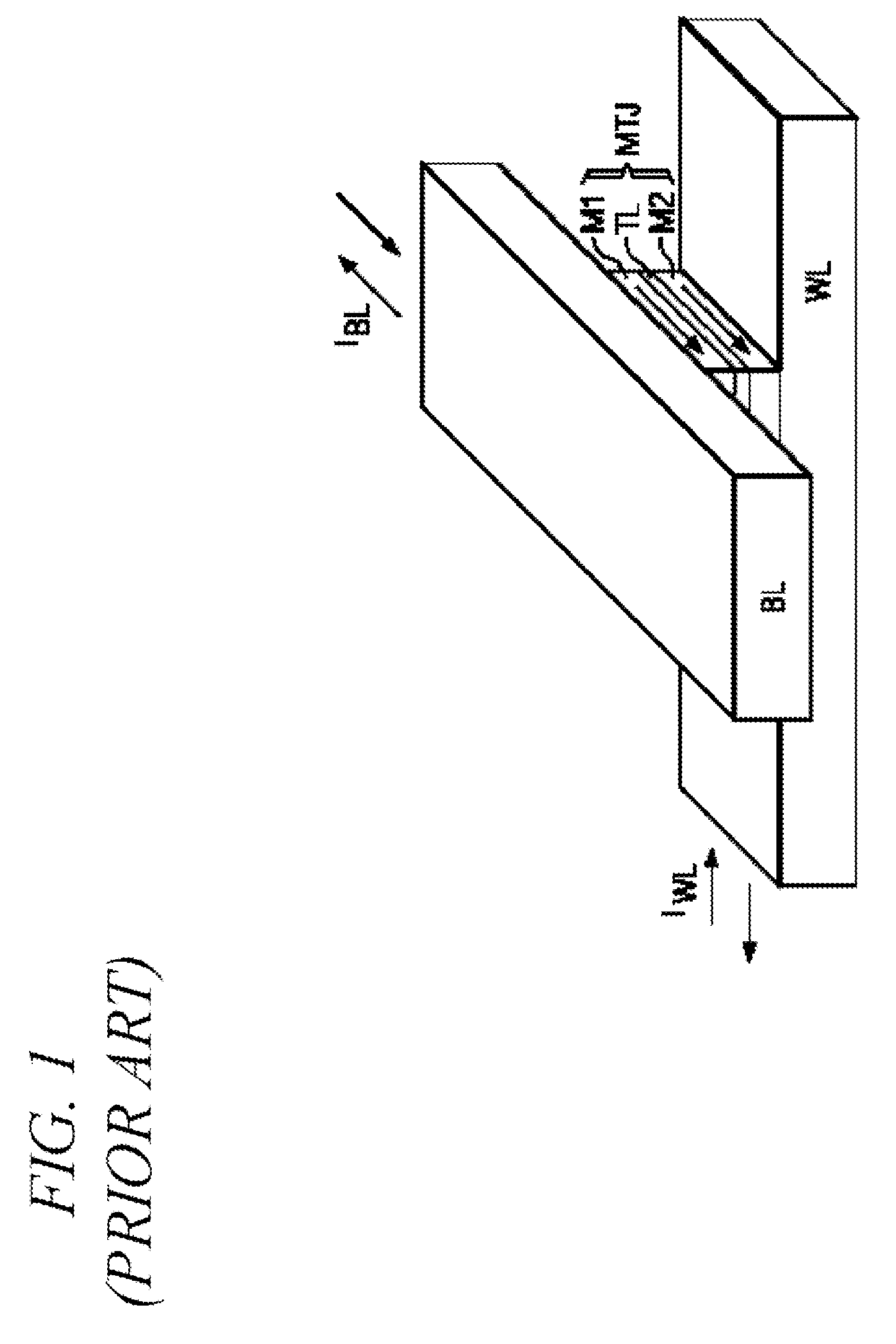
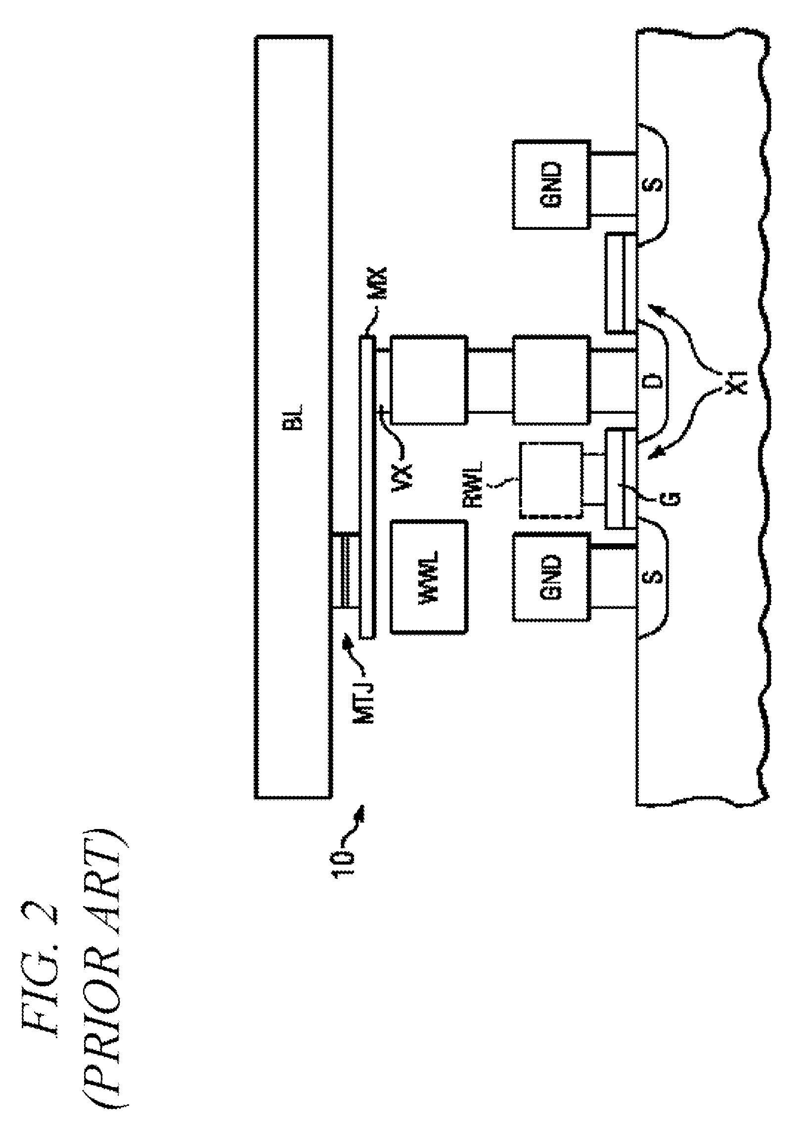
[0047] Embodiments of the present invention will mainly be described with respect to embodiments in a specific context, namely a FET MRAM device. The invention may also be applied, however, to resistive memory devices and other memory devices that use a current sense amplifier to detect the resistive state of memory cells. For example, other embodiments of the present invention are described below in the context of other memory devices such as, for example, PCRAM devices, CBRAM devices, or flash memory devices. The current sense amplifier is also applicable in other applications where an...


PUM


Abstract

An integrated circuit has a current sense amplifier that includes a voltage comparator having a first input, a second input and an output; a first clamping device coupled between the first input of the voltage comparator and a first input signal node, a second clamping device coupled between the second input of the voltage comparator and a second input signal node, a current mirror having a first side and a second side, the current mirror first side including a first transistor coupled between a voltage source and the first clamping device and the current mirror second side including a second transistor coupled between the voltage source and the second clamping device, and a sensing scheme including an actively balanced capacitance coupled to the source and drain of the second transistor.

Description

CROSS-REFERENCE TO RELATED APPLICATIONS [0001] This application is a continuation-in-part application of commonly assigned patent application Ser. No. 10 / 937,155, filed Sep. 7, 2004, which relates to commonly assigned patent application Ser. No. 10 / 326,367, filed Dec. 20, 2002, now issued as U.S. Pat. No. 6,946,882, entitled “Current Sense Amplifier,” which application is hereby incorporated herein by reference.TECHNICAL FIELD [0002] Embodiments of the present invention relate generally to semiconductor memory devices, and more particularly to sensing circuits for determining the resistive state of memory cells. BACKGROUND [0003] Semiconductors are used in integrated circuits for electronic applications, including radios, televisions, cell phones, and personal computing devices, as examples. One type of semiconductor device is a semiconductor storage device, such as a dynamic random access memory (DRAM) and flash memory, which uses a charge to store information. [0004] Various memor...

Claims


Application Information

Patent Timeline
IPC IPC(8): G11C7/10G01R19/00
CPCG11C5/02G11C2213/79G11C7/067G11C11/15G11C11/5614G11C11/5664G11C11/5678G11C13/00G11C13/0004G11C13/0011G11C13/0014G11C13/004G11C2013/0054G11C2207/063G11C2213/71G11C5/04G11C11/1673
Inventor GOGL, DIETMARVIEHMANN, HANS-HEINRICH
Owner POLARIS INNOVATIONS
Why Eureka
Try Eureka