Method of manufacturing semiconductor device

a manufacturing method and semiconductor technology, applied in the direction of semiconductor devices, basic electric elements, electrical appliances, etc., can solve the problems of semiconductor film contamination, reduced throughput, waste of most of the resist material, etc., and achieve high mass productivity, high integration

Inactive Publication Date: 2008-01-31
SEMICON ENERGY LAB CO LTD
View PDF75 Cites 67 Cited by
  • Summary
  • Abstract
  • Description
  • Claims
  • Application Information

AI Technical Summary

Benefits of technology

[0018]Further, when the light absorbing layer is irradiated with a laser beam with a large beam spot area, such as a linear laser beam, a rectangular laser beam, a plane laser beam, or the like, a plurality of regions of the light absorbing layer can be irradiated with a laser beam in a short time; thus, semiconductor devices can be manufactured with high mass productivity.
[0019]Further, when the light absorbing layer is a semiconductor layer, a semiconductor layer having a desired shape can be formed over a substrate while preventing mixing of an impurity element into the semiconductor film due to resist coating, and a semiconductor element can be formed by using

Problems solved by technology

However, in steps of forming wirings, semiconductor layers, insulating layers, using a conventional photolithography process, most of the material of a resist is wasted, and further, the number of steps of forming a wiring, a semiconductor layer, and an insulating layer, or the like is large; thus, throughput is reduced.
At that time, there is a problem in that the

Method used


Image

  • Method of manufacturing semiconductor device
  • Method of manufacturing semiconductor device
  • Method of manufacturing semiconductor device

Examples


embodiment mode 1

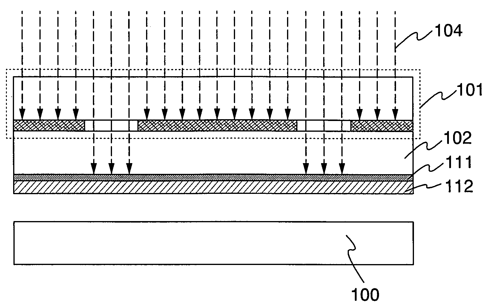
[0054]In this embodiment mode, steps of selectively forming a layer having a given shape over a substrate without using a photolithography process will be described below. FIGS. 1A to 4C are cross-sectional views illustrating steps of selectively forming a layer over a substrate.

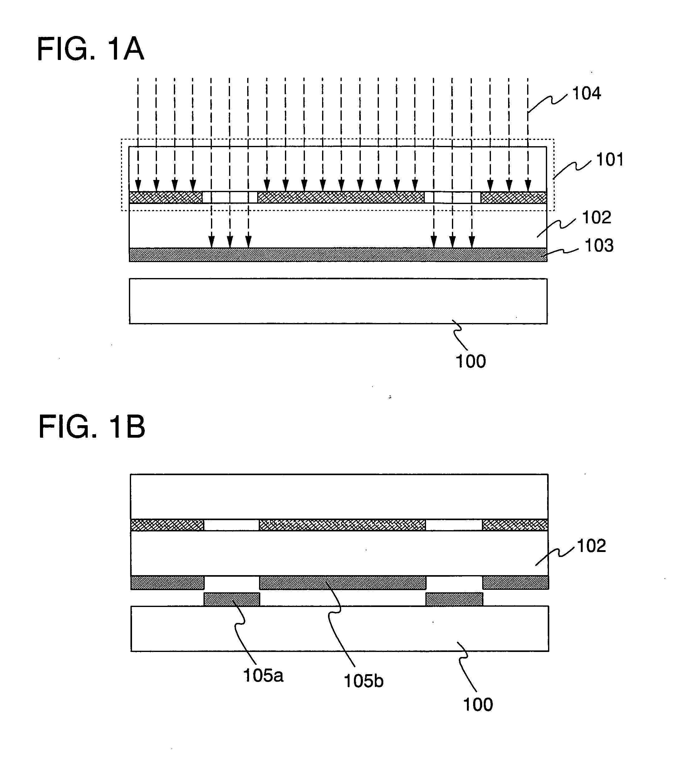
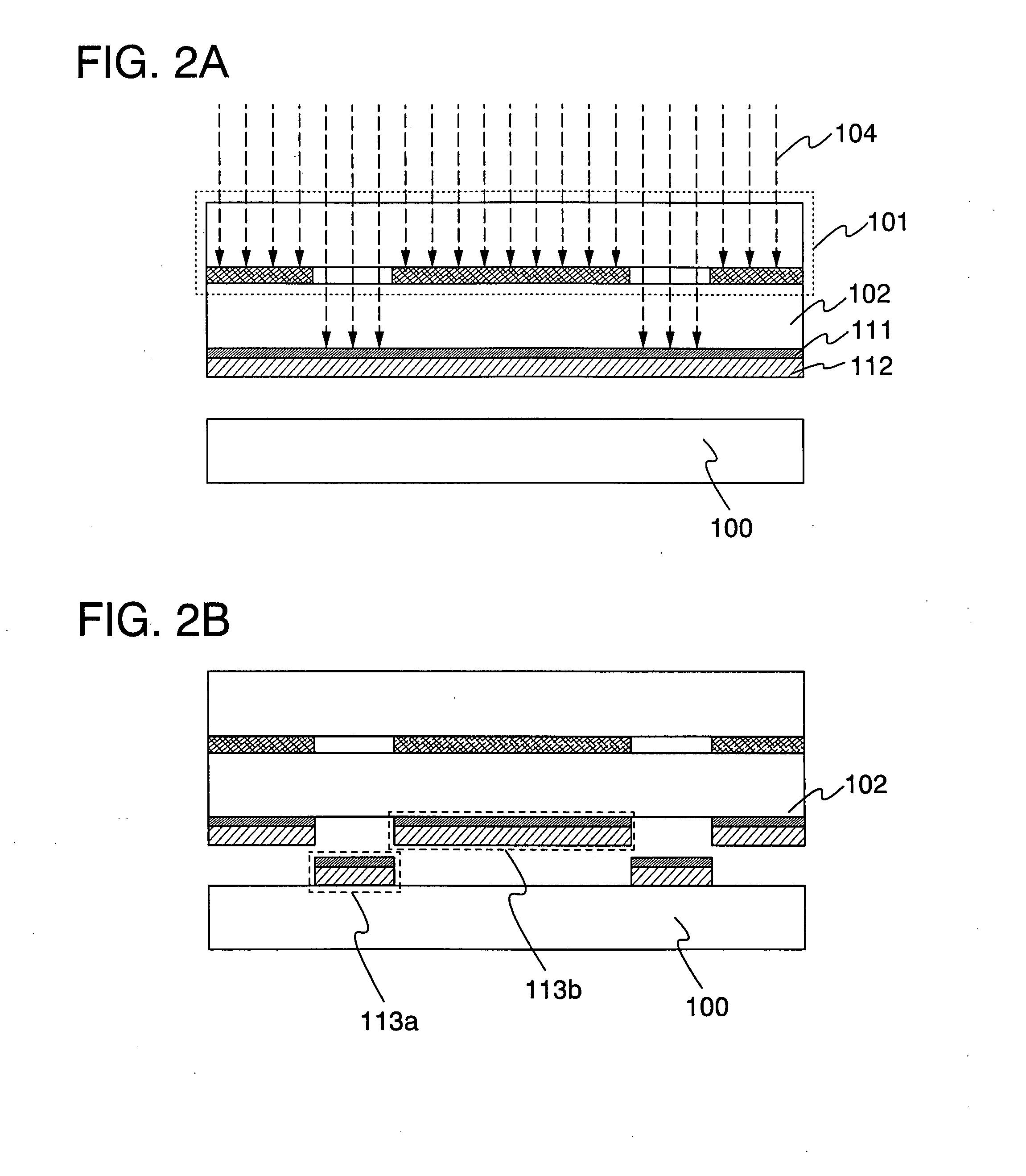
[0055]As shown in FIG. 1A, a light absorbing layer 103 is formed over one face of a light-transmitting substrate. Further, a mask 101 is provided on the other face side of the light-transmitting substrate 102. A substrate 100 is provided so as to oppose the light absorbing layer 103. Note that the one face and the other face of the light-transmitting substrate 102 oppose each other.

[0056]A substrate which transmits light of a laser beam to be applied later can be used as the light-transmitting substrate 102. Accordingly, a substrate which does not absorb the wavelength of the laser beam to be formed later may be used as appropriate. As typical examples of the light-transmitting substrate 102, there are a qua...

embodiment mode 2

[0129]In this embodiment mode, a method of manufacturing a semiconductor element using Embodiment Mode 1 will be described with reference to FIGS. 12A to 12F.

[0130]Here, as the semiconductor element, an inverted staggered thin film transistor 188 will be described. Note that a semiconductor element such as a staggered thin film transistor, a coplanar thin film transistor, a diode, a MOS transistor, or the like can be manufactured without limitation to an inverted staggered thin film transistor.

[0131]As shown in FIG. 12A, a light absorbing layer 181 is formed over one face of a light-transmitting substrate 102. Here, as the light absorbing layer 181, a tungsten layer is formed to a thickness of 10 nm to 1000 nm or more over the light-transmitting substrate 102 by sputtering. Further, a substrate 100 is provided so as to oppose the light absorbing layer 181. A mask 101 is provided on the other face side of the light-transmitting substrate. Note that the one face and the other face of ...

embodiment mode 3

[0146]In this embodiment mode, a method for forming a contact hole through a more simplified process with high reliability at low cost will be described with reference to FIGS. 13A to 14D.

[0147]When conductive layers are electrically connected to each other with an insulating layer interposed therebetween, an opening (so-called contact hole) is formed in the insulating layer. In this case, a mask layer is not formed over the insulating layer, and the opening is selectively formed by laser beam irradiation. A first conductive layer is formed, an insulating layer is stacked over the first conductive layer, and a region where the opening is formed in the stacked first conductive layer and insulating layer is selectively irradiated with a laser beam from the insulating layer side. When the first conductive layer is formed of a conductive material which absorbs a laser beam, the laser beam is transmitted through the insulating layer and absorbed by the first conductive layer. The first c...


PUM


Abstract

A method of forming a semiconductor device is provided, including a step of forming a layer which absorbs light over one face of a first substrate, a step of providing a second substrate over the layer which absorbs light, a step of providing a mask to oppose the other face of the first substrate, and a step of transferring the part of the layer which absorbs light to the second substrate by irradiating the layer which absorbs light with a laser beam through the mask.

Description

BACKGROUND OF THE INVENTION[0001]1. Field of the Invention[0002]The present invention relates to a method of manufacturing a layer such as a conductive layer, semiconductor layer, or an insulating layer, which is formed by a transfer method using a laser beam, or the like. Further, the invention relates to a semiconductor device having a semiconductor element, which is formed using such layers.[0003]2. Description of the Related Art[0004]Conventionally, a so-called active matrix drive display panel or a semiconductor integrated circuit each of which has a semiconductor element typified by a thin film transistor (hereinafter also referred to as a “TFT”) or a MOS transistor is manufactured by forming a resist mask through light-exposure steps using a photomask (hereinafter referred to as a photolithography process) and then selectively etching each thin film.[0005]In a photolithography process, a resist mask is formed by coating the entire surface of a substrate with a resist, prebaki...

Claims


Application Information

Patent Timeline
IPC IPC(8): H01L21/30
CPCH01L27/1266H01L29/66765H01L27/1288H01L21/0274
Inventor MIYAIRI, HIDEKAZUSHOJI, HIRONOBUSHIMOMURA, AKIHISAHIGA, EIJIMORIWAKA, TOMOAKIYAMAZAKI, SHUNPEI
Owner SEMICON ENERGY LAB CO LTD
Why Eureka
Try Eureka