Low-noise single-gate non-volatile memory and operation method thereof

a non-volatile memory, low-noise technology, applied in the direction of semiconductor devices, electrical devices, transistors, etc., can solve the problems of increasing the cost of operation after voltage booster, and increasing the difficulty and cost of fabrication, so as to achieve the effect of reducing the current for programming the single-gate non-volatile memory and facilitating the flow of current to the floating ga

Inactive Publication Date: 2008-02-14
YIELD MICROELECTRONICS CORP
View PDF3 Cites 27 Cited by
  • Summary
  • Abstract
  • Description
  • Claims
  • Application Information

AI Technical Summary

Benefits of technology

[0007]The primary objective of the present invention is to provide a low-noise single-gate non-volatile memory and an operation method thereof, wherein two electrically-conductive gates are electrically connected to form single-floating-gate structure; in programming the memory, a really active voltage is applied to the source, or a back bias is applied to the transistor substrate, in order to create a wider depleted source-substrate junction; thereby, current can flow to the floating gate more efficiently, and the current for programming the single-gate non-volatile memory can be greatly reduced.

Problems solved by technology

In the conventional non-volatile memories, the operation voltage is usually over 10 volts; thus, not only the required voltage boostering circuit increases the cost, but also the operation after voltage booster consumes considerable current.
Further, when the conventional non-volatile memories, especially embedded products, are fabricated with an advanced process, it usually needs many extra procedures, which increases the difficulties and cost of fabrication.

Method used


Image

  • Low-noise single-gate non-volatile memory and operation method thereof
  • Low-noise single-gate non-volatile memory and operation method thereof
  • Low-noise single-gate non-volatile memory and operation method thereof

Examples


first embodiment

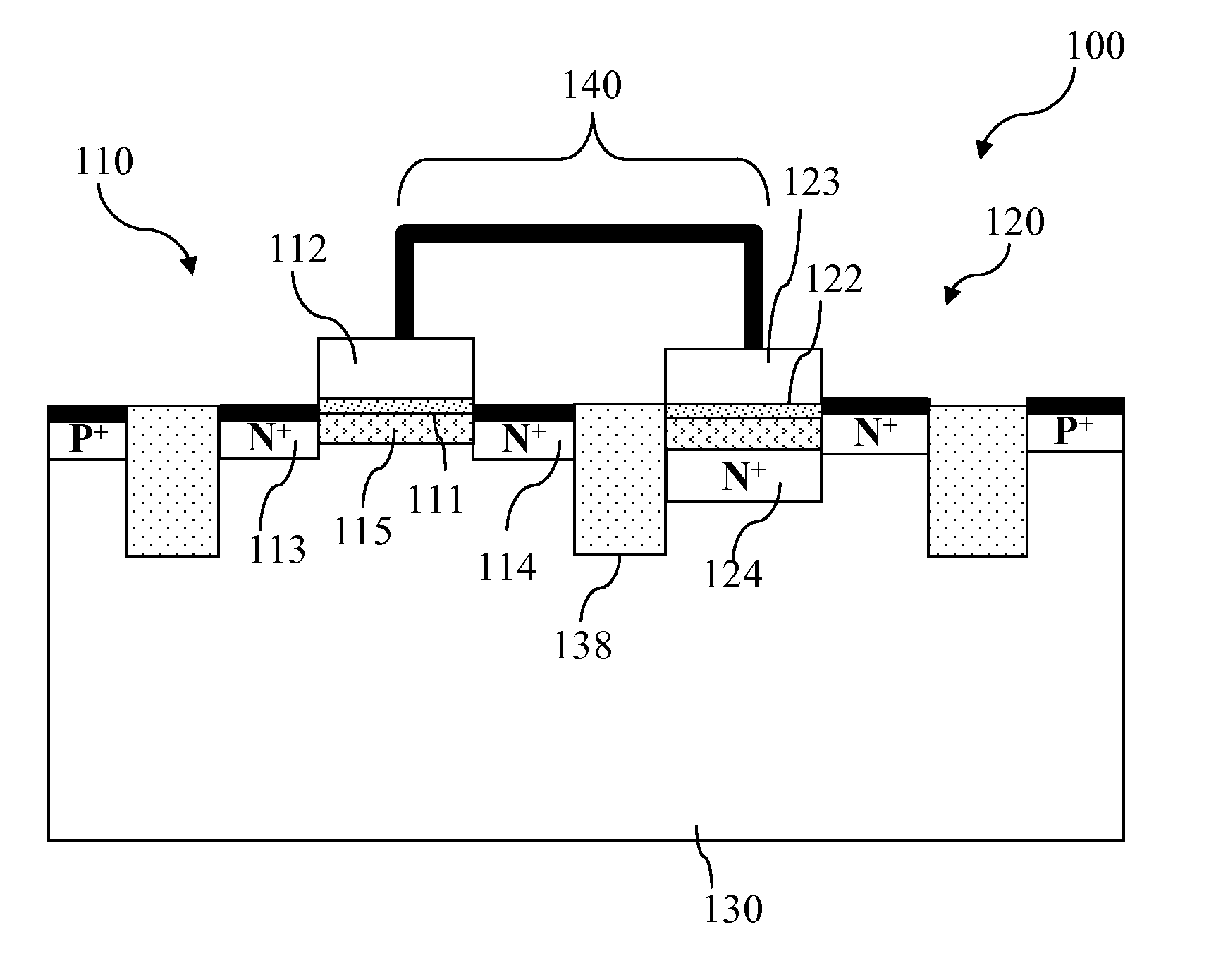
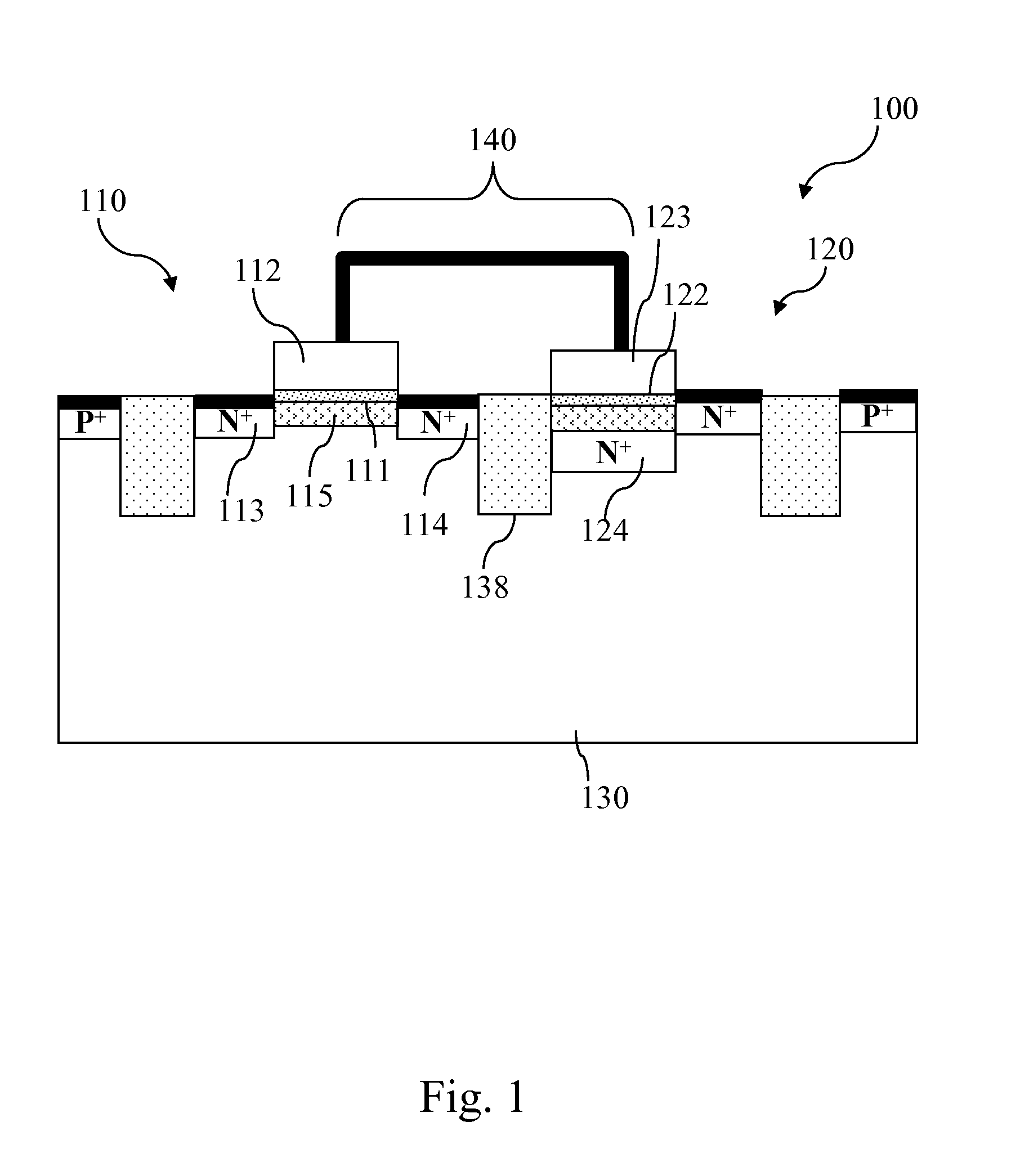
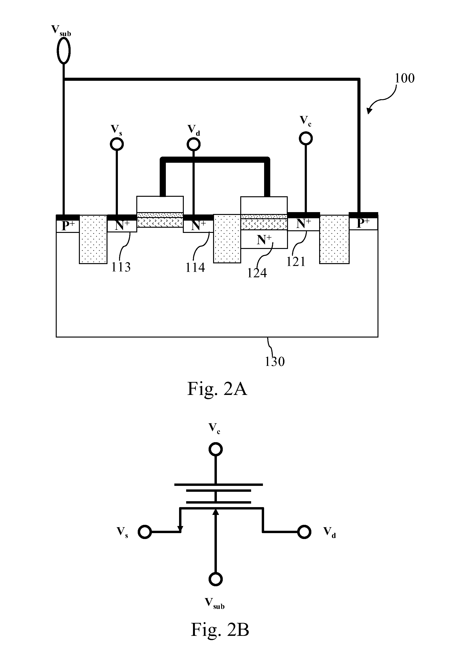
[0025]Refer to FIG. 1 a sectional view schematically showing the structure of the low-noise single-gate non-volatile memory according to the present invention. The low-noise single-gate non-volatile memory structure 100 comprises: an NMOS transistor (NMOSFET) 110 and an N-type capacitor structure 120 with both of them embedded in a P-type semiconductor substrate 130. The NMOS transistor 110 further comprises: a first dielectric layer 111, disposed on the surface of the P-type semiconductor substrate 130; a first electrically-conductive gate 112, stacked on the first dielectric layer 111; and two first ion-doped regions, disposed inside the P-type semiconductor substrate 130, and respectively functioning as the source 113 and the drain 114 with a channel 115 formed between the source 113 and the drain 114. The N-type capacitor structure 120 further comprises: a second ion-doped region 121 and a second ion-doped buried layer 124, respectively disposed in the P-type semiconductor subst...

second embodiment

[0031]Refer to FIG. 3 a sectional view schematically showing the structure of the low-noise single-gate non-volatile memory according to the present invention. The low-noise single-gate non-volatile memory structure 200 comprises: a PMOS transistor 210 and an N-type capacitor structure 220 with both of them embedded in a P-type semiconductor substrate 230. The first ion-doped regions of the PMOS transistor 210 are P-type ion-doped regions, and the second ion-doped region 221 and the second ion-doped buried layer 124 of the N-type capacitor structure 220 are N-type ion-doped regions. The low-noise single-gate non-volatile memory structure 200 further comprises an N-type well 216 disposed below the first ion-doped regions. The first electrically-conductive gate 212 of the PMOS transistor 210 and the second electrically-conductive gate 223 on the top of the N-type capacitor structure 220 are also separated with an isolation material 238 and electrically interconnected to form a single ...

third embodiment

[0038]Refer to FIG. 5 a sectional view schematically showing the structure of the low-noise single-gate non-volatile memory according to the present invention. The low-noise single-gate non-volatile memory structure 300 comprises: an NMOS transistor 310, an N-type capacitor structure 320, and a P-type well 317 with all of them embedded in an N-type semiconductor substrate 330. The NMOS transistor 310 and the N-type capacitor structure 320 are disposed on the surface of the P-type well 317. The first electrically-conductive gate 312 of the NMOS transistor 310 and the second electrically-conductive gate 323 on the top of the N-type capacitor structure 320 are also separated with an isolation material 338 and electrically interconnected to form a single floating gate 340.

[0039]When the writing and erasing processes of the low-noise single-gate non-volatile memory structure 300 are undertaken, a P-type well voltage Vpwell, a source voltage Vs, a drain voltage Vd, a control gate voltage ...


PUM


Abstract

The present invention discloses a low-noise single-gate non-volatile memory and an operation method thereof, wherein a transistor and a capacitor structure are embedded in a semiconductor substrate; the electrically-conductive gate of the transistor and the electrically-conductive gate of the capacitor structure are interconnected to form a single floating gate of a memory cell; an ion-doped buried layer is formed between the dielectric layer of the capacitor structure and the semiconductor substrate to reduce the external interference on the capacitor structure and control the initial threshold voltage; a reverse bias may be used to implement the reading, writing, and erasing operations of the single-floating-gate memory cell; in the operation of the low-noise single-gate non-volatile memory having an isolation well, positive and negative voltages may be applied to the drain, the gate, and the silicon substrate/the isolation well to create an inversion layer, and thereby, the absolute voltage, the area of the voltage booster circuit, and the current consumption can be reduced.

Description

BACKGROUND OF THE INVENTION[0001]1. Field of the Invention[0002]The present invention relates to a non-volatile memory and an operation method thereof, particularly to a low-noise single-gate non-volatile memory and an operation method thereof, wherein the memory can be written or erased with a low voltage and a low current consumption.[0003]2. Description of the Related Art[0004]The CMOS (Complementary Metal Oxide Semiconductor) process has been a common fabrication method for ASIC (Application Specific Integrated Circuit). EEPROM is the abbreviation of Electrically Erasable Programmable Read Only Memory. In EEPROM, data not only can be electrically written and erased but also will not volatilize after power has been turned off; therefore, EEPROM has been extensively used in electronic products.[0005]A non-volatile memory is programmable. In principle, whether the gate voltage is changed or maintained depends on the charging state. In erasing a non-volatile memory, the charges stor...

Claims


Application Information

Patent Timeline
Patent Type & Authority Applications(United States)
IPC IPC(8): H01L29/94
CPCH01L27/115H01L27/11558H01L27/11521H10B41/60H10B69/00H10B41/30
Inventor LIN, HSIN CHANGHUANG, WEN CHIENCHANG, HAO CHENGWU, CHENG YINGYANG, MING TSANG
Owner YIELD MICROELECTRONICS CORP
Why Eureka
Try Eureka