Unit-Layer Post-Processing Catalyst Chemical-Vapor-Deposition Apparatus and Its Film Forming Method

a unit-layer post-processing catalyst and chemicalvapor-deposition technology, which is applied in chemical vapor-deposition coatings, vacuum evaporation coatings, coatings, etc., can solve the problems of insufficient step coverage, insufficient in-face film thickness, and in-face film thickness uniformity of conventional cvd, so as to improve in-face film thickness uniformity, step coverage, and film quality.

Inactive Publication Date: 2008-02-28
ULVAC INC
View PDF8 Cites 23 Cited by
  • Summary
  • Abstract
  • Description
  • Claims
  • Application Information

AI Technical Summary

Benefits of technology

[0027]Since a unit-layer post-processing catalyst vapor-deposition apparatus of the present invention can change gas introduction at once, it has advantages that it is possible to form a film for each unit layer, perform surface treatment for each formed unit layer, and improve in-face film-thickness uniformity, step coverage, and film quality.
[0028]Moreover, a unit-layer post-processing film forming method of the present invention has an advantage that it is possible to form a laminated thin film in which the in-face uniformity of a film thickness, step coverage, and film quality are improved because surface treatment is performed after film formation for each unit layer.

Problems solved by technology

However, a silicon-nitride film formed by the conventional CVD method like one disclosed in the above Patent Document 1 does not have a good in-face uniformity of a film thickness and is insufficient in step coverage and a film having a good current-voltage (I-V) withstand-voltage characteristic is not obtained.

Method used


Image

  • Unit-Layer Post-Processing Catalyst Chemical-Vapor-Deposition Apparatus and Its Film Forming Method
  • Unit-Layer Post-Processing Catalyst Chemical-Vapor-Deposition Apparatus and Its Film Forming Method
  • Unit-Layer Post-Processing Catalyst Chemical-Vapor-Deposition Apparatus and Its Film Forming Method

Examples


example 1

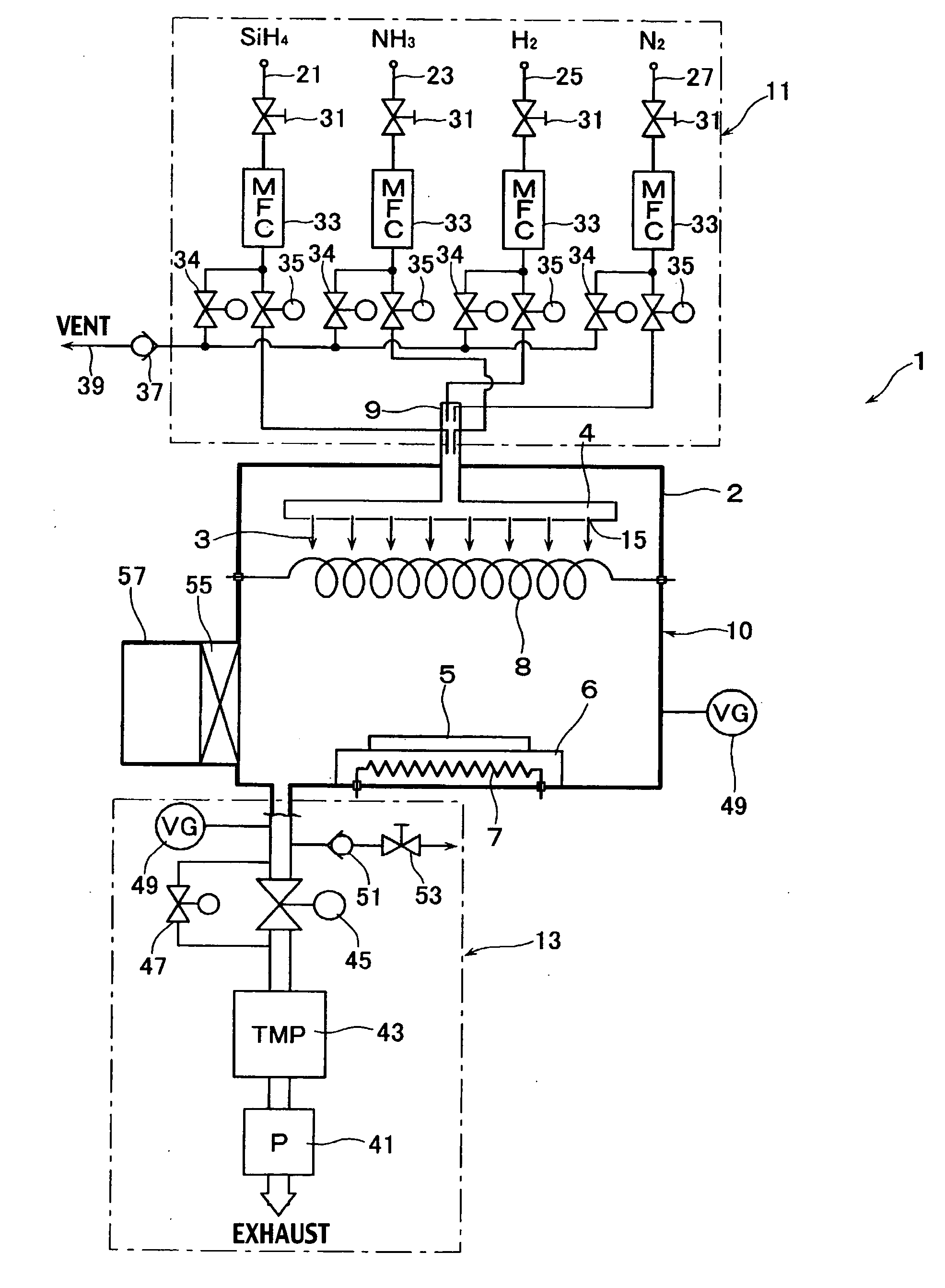
[0192]As shown in FIG. 1, in the case of Example 1, a heater 7 is electrified and resistance-heated under a reduced pressure of 10 Pa, a substrate 5 on a substrate holder 6 is heated up to, for example, 200° C., a catalyst body (such as tungsten thin wire) 8 is electrified and resistance-heated up to 1,700° C.

[0193]As film forming conditions, the flow rate of silane gas (SiH4) is 7 sccm, flow rate of ammonia gas (NH3) is 10 sccm, flow rate of hydrogen gas (H2) is 10 sccm, pressure in the reactive vessel 2 is 10 Pa, and temperature of the catalyst body 8 is 1,700° C. as shown in FIG. 19. In the case of this example, a very-thin silicon nitride film having a thickness of 1 nm is obtained.

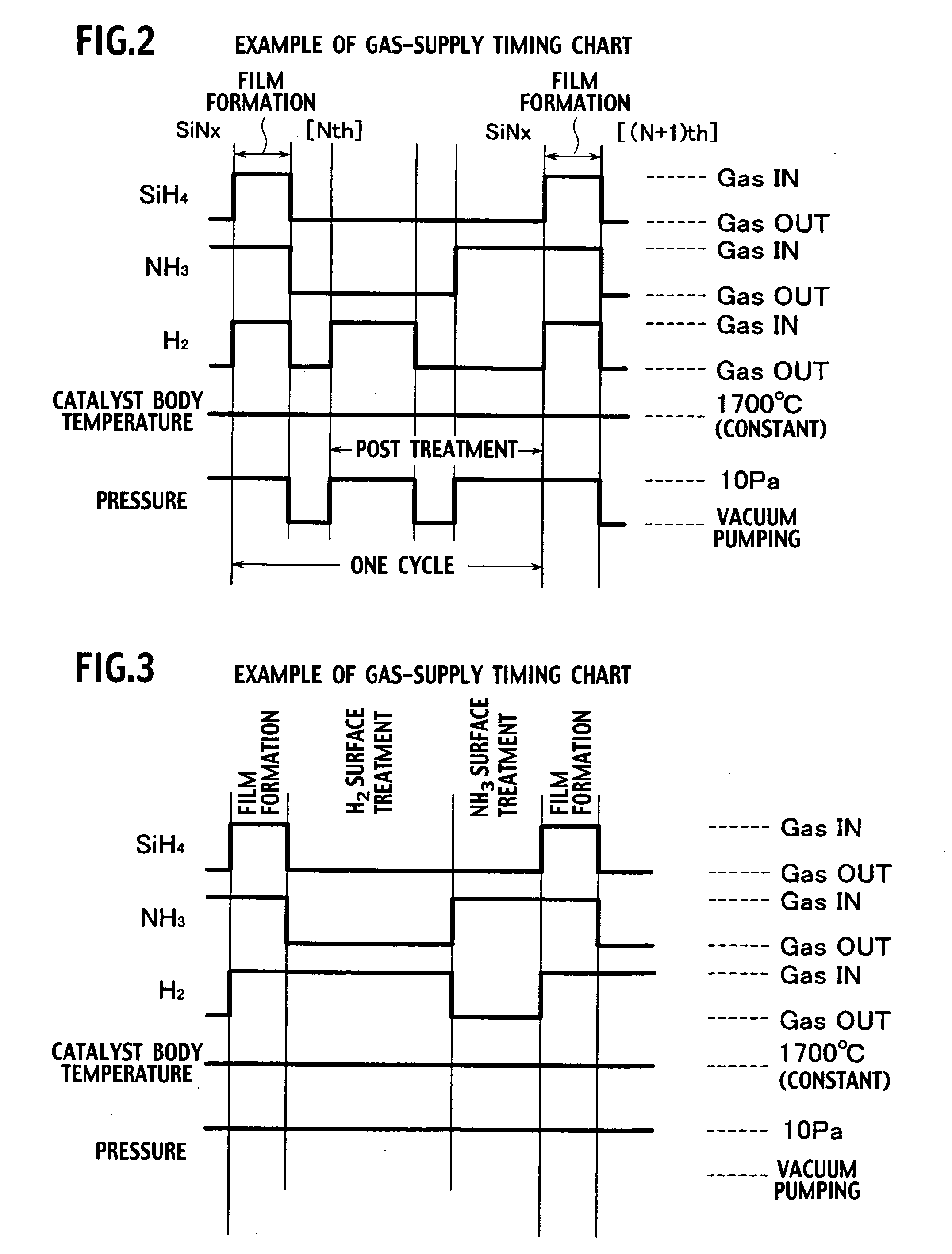
[0194]In the timing chart shown in FIG. 2, a silicon nitride film having the total thickness of 50 nm is finally obtained by using a film forming step and one and other surface treating steps as one cycle and continuously repeating the film forming step of one cycle and one and other surface treating ...

example 2

[0200]In the case of the Example 1, a silicon nitride film having a thickness of 50 nm is finally formed by forming a silicon nitride film having a thickness of 1 nm in one film forming step and continuously repeating one-cycle step of the film forming step and one and other surface treating steps 50 times. In the case of the Example 2, however, a silicon nitride film having a thickness of 1 nm is formed in a step of one cycle by the film forming method same as the case of the Example 1 and a silicon nitride film having a thickness of 100 nm is finally formed by continuously repeating the surface treatment step of one cycle 100 times.

[0201]In the case of step film forming conditions in this time, as shown in FIG. 20, the flow rate of silane gas (SiH4) is 7 sccm, flow rate of ammonia gas (NH3) is 10 sccm, flow rate of hydrogen gas (H2) is 10 sccm, pressure in the reactive vessel 2 is 10 Pa, and temperature of the catalyst body 8 is 1,700° C. (these conditions are the same as the case...

example 3

[0207]In the case of Example 3, a silicon nitride film having a thickness of 1 nm is formed through one-time film forming step by the film forming method same as the case of the Example 2 and a silicon nitride film having a thickness of 100 nm is finally formed by continuously repeating the film forming step, one surface treating step, and other surface treating step 100 times.

[0208]In the case of film forming conditions in this case, as shown in FIG. 22, the flow rate of silane gas (H2) is 7 sccm, flow rate of ammonia gas (HN3) is 10 sccm, flow rate of hydrogen gas (H2) is 10 sccm, pressure of the reactive vessel 2 is 10 Pa, and temperature of the catalyst body 8 is 1,700° C. (these conditions are the same as the case of the film forming method of the embodiment 2) and a very-thin silicon nitride film having a thickness of 1 nm is obtained in one-time film forming step for 10 sec in this case in the case of the Example 3.

[0209]Then, as a result of measuring the in-face uniformity o...


PUM

PropertyMeasurementUnit
temperatureaaaaaaaaaa
thicknessaaaaaaaaaa

Abstract

To provide a unit-layer post-treatment catalyst vapor-deposition apparatus and unit-layer post-treatment film forming method capable of improving in-face uniformity, step coverage, and film quality of a silicon nitride film or the like and forming a thin film by performing surface treatment after forming a film for each unit layer.
A thin film post-treated for each unit layer is laminated by using a film forming step of introducing mixed gas of silane gas and ammonia gas into a reactive vessel 2 as a source gas like a rectangular pulse and contacting with and thermal-decomposing the source gas by a catalyst body 8, and forming a silicon nitride film on a substrate 5, one surface treating step of bringing ammonia gas into contact with the catalyst body 8 and then bleaching the ammonia gas on the surface of a silicon nitride film on the substrate 5 and other surface treating step of bleaching hydrogen gas on the surface of the silicon nitride film on the substrate 5 after bringing hydrogen gas into contact with the catalyst body 8 as one cycle and repeating the step of one cycle.

Description

TECHNICAL FIELD[0001]The present invention relates to a unit-layer post-processing catalyst chemical-vapor-deposition apparatus according to a catalyst chemical vapor deposition method for forming a film every unit layer and then surface-treating and laminating the thin films and its film forming method.BACKGROUND ART[0002]Various types of semiconductor devices, a liquid-crystal display (LCD) and the like are respectively fabricated by forming a predetermined thin film on a substrate. As the film forming method, a CVD method (also referred to as chemical vapor growth method or chemical vapor deposition method) has been used so far, for example.[0003]As the CVD method, heat CVD method, plasma CVD method and the like have been known so far. Recently, however, a catalyst CVD method (also referred to as Cat-CVD method or hot-wire CVD method) has been practically used which forms a deposited film on a substrate by using an element wire made of heated tungsten or the like (hereafter refer...

Claims


Application Information

Patent Timeline
Patent Type & Authority Applications(United States)
IPC IPC(8): C23C16/00C23C14/00C23C16/34C23C16/42C23C16/44C23C16/56H01L21/318
CPCC23C16/345H01L21/3185C23C16/45523C23C16/44H01L21/02277H01L21/022H01L21/0228H01L21/0217H01L21/02337
Inventor KITAZOE, MAKIKOITHO, HIROMIASARI, SHINSAITO, KAZUYA
Owner ULVAC INC
Why Eureka
Try Eureka