Method for Making Electrically Conductive Three-Dimensional Structures

a three-dimensional structure and electrically conductive technology, applied in the field of micro-scale structures, can solve the problems of inability to scale to larger production, inability to make larger-scale production, and additional challenges in patterning high-aspect-ratio three-dimensional structures

Inactive Publication Date: 2008-03-13
GEORGIA TECH RES CORP
View PDF14 Cites 87 Cited by
  • Summary
  • Abstract
  • Description
  • Claims
  • Application Information

AI Technical Summary

Benefits of technology

[0018] Methods are also provided for making microneedle arrays. In one embodiment, the method includes the steps of providing a mold having at least one microdepression which defines a high-aspect ratio three-dimensional structure; depositing and patterning at least one electrically conductive layer within microdepression of the mold; filling the microdepression of the mold with at least one substrate material; molding the at least one substrate material to form a substrate on top of the at least one electrically conductive layer; and transferring the at least one electrically conductive layer to the substrate, thereby forming a high-aspect ratio, electrically conductive array structure.

Problems solved by technology

While conventional structures have been created through well-known techniques such as micromachining of solid conductors, these approaches are not cost-effective and therefore cannot be scaled to larger production.
Although electrodeposition may provide cost savings over micromachining of solid conductive structures, an additional challenge exists in patterning high-aspect-ratio three-dimensional structures due to difficulty in non-planar surface patterning using conventional lithographic approaches.

Method used


Image

  • Method for Making Electrically Conductive Three-Dimensional Structures
  • Method for Making Electrically Conductive Three-Dimensional Structures
  • Method for Making Electrically Conductive Three-Dimensional Structures

Examples


example 1

Microneedle Fabrication

[0063] A microneedle device including a 16×16 array of electrically active microneedles was fabricated with adjacent microneedle rows electrically isolated. The height of the microneedles was 400 μm, bottom diameter was 100 μm, and pitch between microneedles was 250 μm.

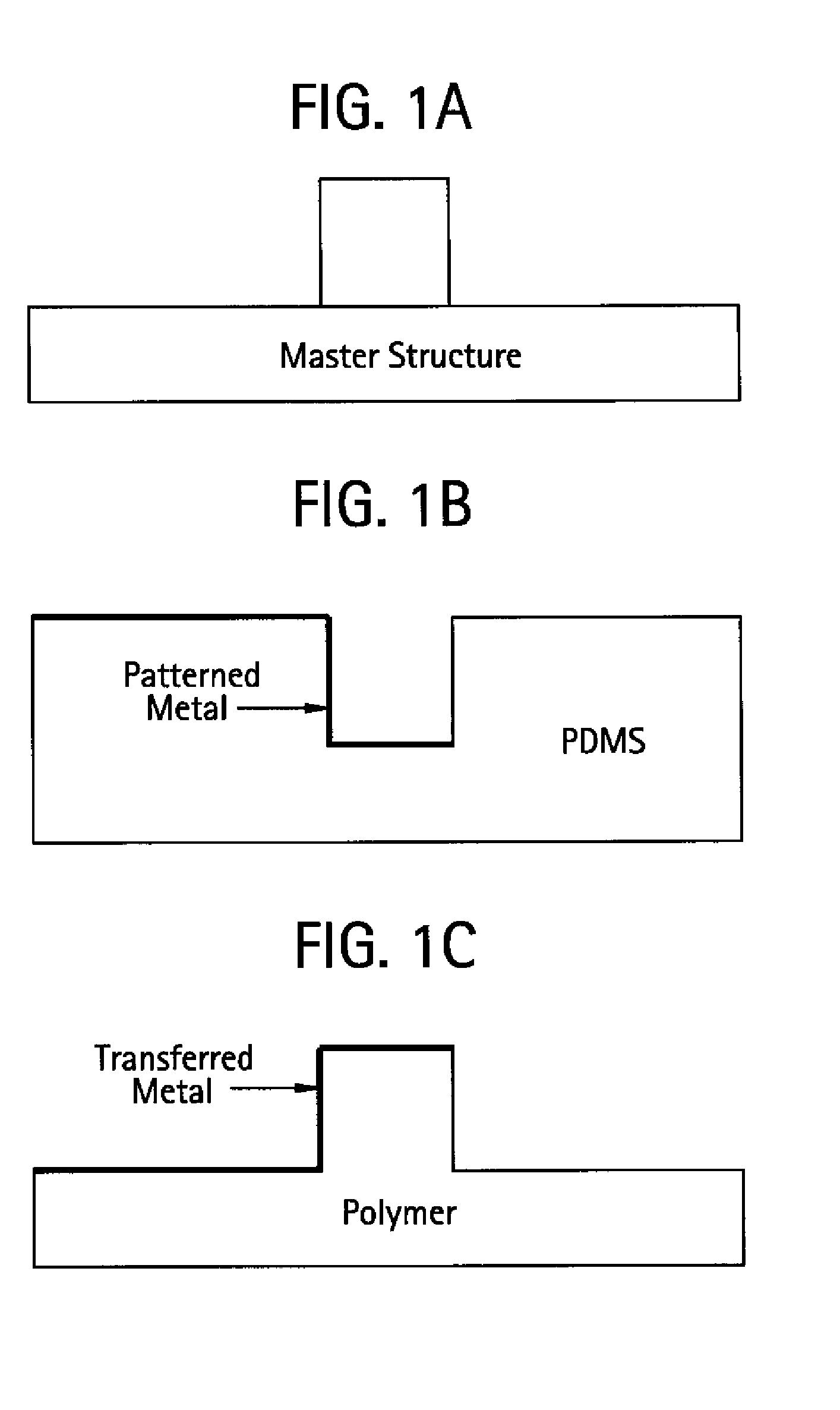
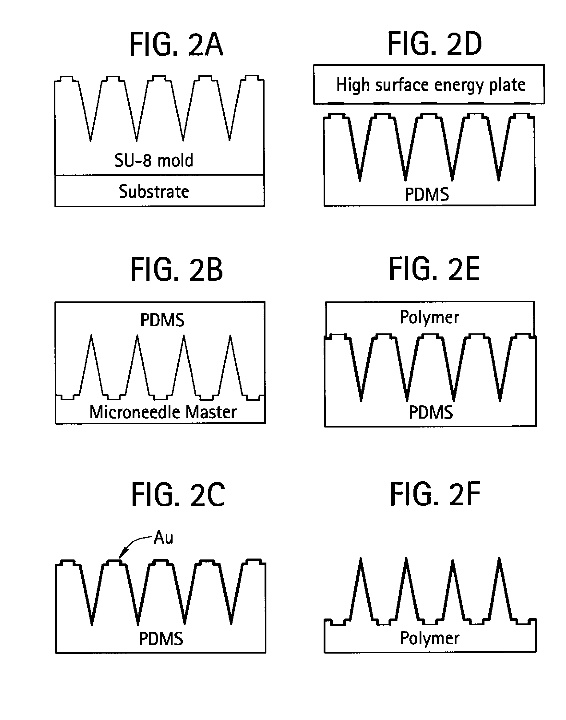
[0064] The microneedle device was fabricated by mold replication from a micromachined master. To fabricate the master structure, SU-8 was spun on a glass substrate bearing an array mask pattern, baked, and then exposed from the backside to form the tapered needle structure. The microneedles were sharpened by RIE etching. A PDMS (polydimethylsiloxane) mold was copied from the master (FIG. 6A) and a PMMA (polymethylmethacrylate) microneedle array (FIG. 6B) was formed by solvent-casting and then released from the mold.

[0065] The PMMA was prepared from a PMMA powder (MW=75,000, Scientific Polymer Products Inc., USA) dissolved in ethyl 1(−)-lactate (Acros Organics, USA). Due in part to the reducti...

example 2

Mechanical Strength of Microneedle Electrodes

[0068] The microneedle electrodes prepared in Example 1 were analyzed to determine whether their mechanical properties were sufficient for insertion into the skin. The yield stress of the microneedle array to an axial load was determined by using a force-displacement testing station (Tricor Systems, USA). The microneedle array was attached to the specimen holder of the force-displacement test station and then pressed against a rigid metal surface at a rate of 1.1 mm / s. Stress versus strain curves were then extracted from the measured force vs. displacement data. The failure force of the microneedle array also was determined from the force versus displacement data by correlation to a sudden drop in measured force, which represents the failure point. The microneedle array was examined under microscope before and after the test to determine the mode of failure.

[0069] For the solvent-cast PMMA microneedle array, the average failure force pe...

example 3

Electroporation of Microneedle Array

[0072] To test the electroporation ability of the microneedle array, an in vitro red blood cell (RBC) lysis assay was performed to quantify the electroporation effect. Approximately 20 ml of bovine blood in alsevers anticoagulant (Rockland Inc., USA) was measured into a 50 ml polypropylene centrifuge tube. Phosphate buffered saline (PBS) was added to the tube which was then centrifuged at 236 G for 10 minutes. The supernatant was discarded and three 20 ml PBS washes were conducted, the supernatant was discarded, and a resultant RBC pellet was formed.

[0073] The microneedle array was affixed to a surface with the microneedles projecting upward. The array was connected to electrical circuitry to provide a controlled electroporation pulse with an exponential decay waveform (FIG. 7). For each electroporation experiment, 25 μl of concentrated RBC pellet was pipetted onto the microneedle array. Three different peak voltage levels of 53, 108 and 173 vol...


PUM

PropertyMeasurementUnit
thicknessaaaaaaaaaa
temperatureaaaaaaaaaa
thicknessesaaaaaaaaaa

Abstract

Methods are provided for fabricating three-dimensional electrically conductive structures. Three-dimensional electrically conductive microstructures are also provided. The method may include providing a mold having at least one microdepression which defines a three-dimensional structure; filling the microdepression of the mold with at least one substrate material; molding the at least one substrate material to form a substrate; and depositing and patterning of at least one electrically conductive layer either during the molding process or subsequent to the molding process to form an electrically conductive structure. In one embodiment, the three-dimensional electrically conductive microstructure comprises an electrically functional microneedle array comprising two or more microneedles, each including a high aspect ratio, polymeric three dimensional substrate structure which is at least substantially coated by an electrically conductive layer.

Description

CROSS-REFERENCE TO RELATED APPLICATIONS [0001] This application claims benefit of U.S. Provisional Application No. 60 / 809,049, filed May 26, 2006. That application is incorporated herein by reference.STATEMENT REGARDING FEDERALLY SPONSORED RESEARCH OR DEVELOPMENT [0002] This invention was made with U.S. government support under Contract No. 2 R44 AI055212-02 awarded by the National Institute of Health. The U.S. government has certain rights in the invention.FIELD OF THE INVENTION [0003] The present invention relates generally to methods for making electrically functional three-dimensional structures, including high-aspect ratio structures, and more particularly to microscale structures made by applying and patterning electrically conductive layers onto substrates. BACKGROUND OF THE INVENTION [0004] Electrically functional three-dimensional structures have a variety of uses in biomedical, chemical, physical, and electronic applications. Non-limiting examples of these applications inc...

Claims


Application Information

Patent Timeline
Patent Type & Authority Applications(United States)
IPC IPC(8): B32B3/30
CPCA61B5/685Y10T428/2958A61M37/0015A61M2037/0053A61N1/327H05K3/20H05K3/4007H05K2201/0367H05K2201/09045H05K2201/09118H05K2203/0113H01B13/00H05K1/02C25D5/022C25D1/003C25D1/10Y10T428/298A61B2562/125B32B3/30
Inventor ALLEN, MARK G.CHOI, SEONG-OPARK, JUNG-HWANWU, XIAOSONGZHAO, YANZHUYOON, YONG-KYURAJARAMAN, SWAMINATHAN
Owner GEORGIA TECH RES CORP
Why Eureka
Try Eureka