

Decal transfer lithography
a transfer lithography and decal technology, applied in the field of decal transfer lithography, can solve the problems of limited range of materials which can be used as substrates and inks, limit the resolution that can be obtained, and extreme difficulty in applying, removing, and manipulating thin elastomeric membranes
- Summary
- Abstract
- Description
- Claims
- Application Information
AI Technical Summary
Benefits of technology
Problems solved by technology
Method used
Image

Examples
example 1
Mask Preparation
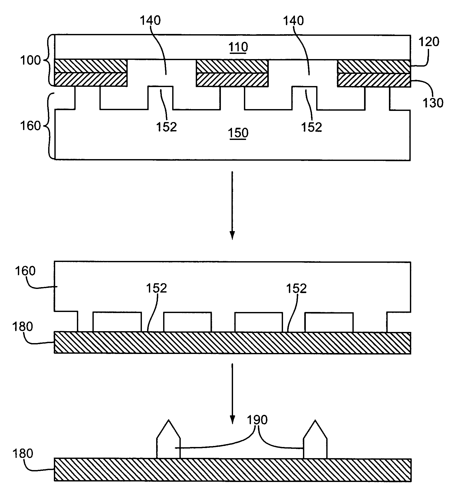
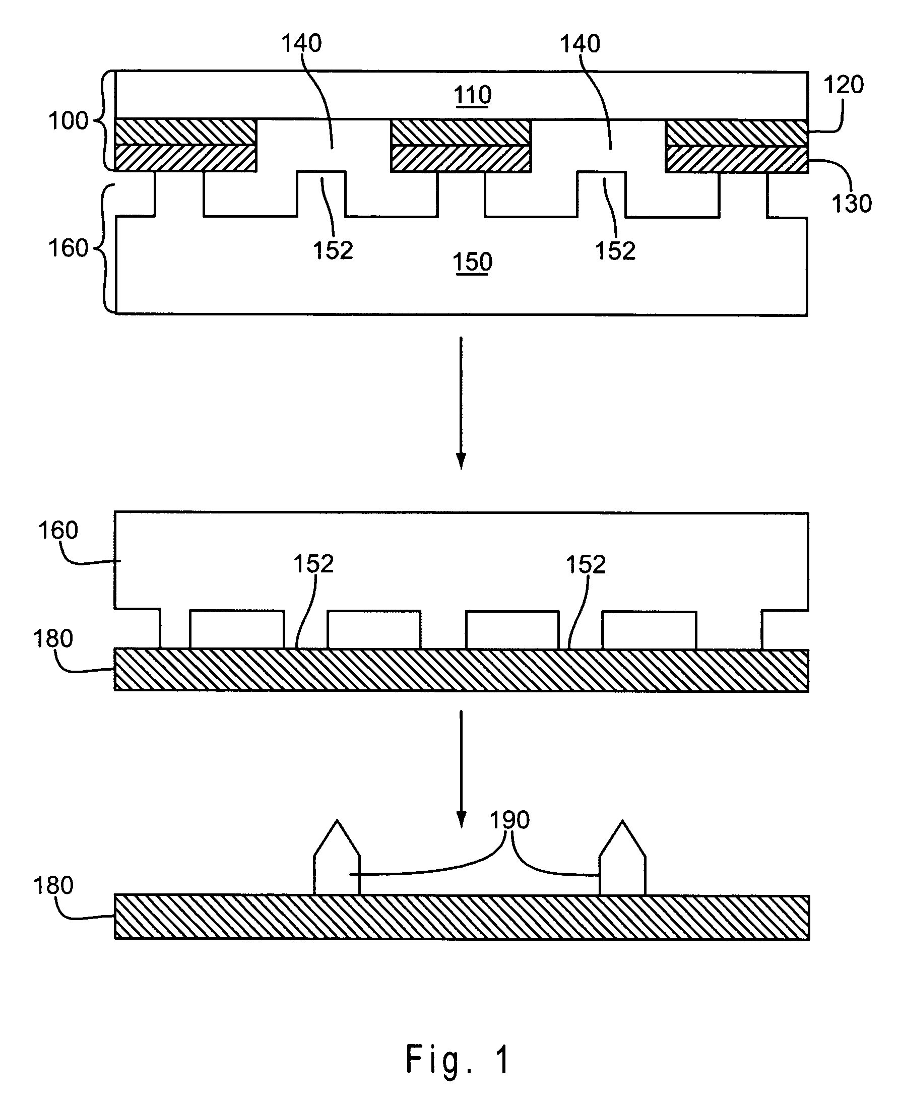
[0071]Quartz slides were cleaned in a piranha solution (3:1 H2SO4:hydrogen peroxide 30%) for 10 min, washed with deionized water and dried with nitrogen. A 30 Å titanium layer and a 1000 Å thick gold film were deposited onto the surface of a quartz slide by evaporation using a TEMESCAL FC-1800 Electron Beam Evaporator (BOC EDWARDS, Wilmington, Mass.). The deposited metal layer was patterned into a square planar array of rectangular cavities having dimensions of 45 microns by 55 microns. This patterning was carried out by contact photolithography using SU8-5 photoresist. The patterned quartz slide was cleaned in an oxygen plasma for 15 s, the exposed gold areas were etched in a dilute (4:1) solution of TFA Gold Etch, and the exposed titanium layer etched by a 1% HF solution. The unstripped layer of the photoresist was retained as part of the final mask, providing a spacer of SU8-5 resist, with a pitch of one. The resist layer had a uniform thickness of 17 μm.
example 2
Patterning Using Photodefined Cohesive Mechanical Failure (P-CMF)
[0072]A molded PDMS stamp was prepared as recommended by DOW CORNING in the SYLGARD 184 kit, by mixing the oligomer and initiator in a 10:1 ratio. The recommended procedure was modified by reducing the pressure (50 torr) at room temperature for several minutes with a vacuum oven to remove entrained gas bubbles. The prepolymer mixture was cast onto a master, and, after waiting 10 min for the mixture to level, the mixture was cured at 70° C. for two hours. The patterned PDMS elastomer was then extracted from the master, washed with ethanol, and dried under a stream of high purity nitrogen to provide the PDMS stamp. The final PDMS stamp had a pattern of a square array of posts, 2 μm in diameter with a center-to-center separation of 2.7 μm.
[0073]The PDMS stamp was placed into contact with the patterned side of the UVO photomask of Example 1 and irradiated through the mask for 4 minutes using a deuterium lamp. The mask was ...
example 3
Use of P-CMF Pattern as Resist
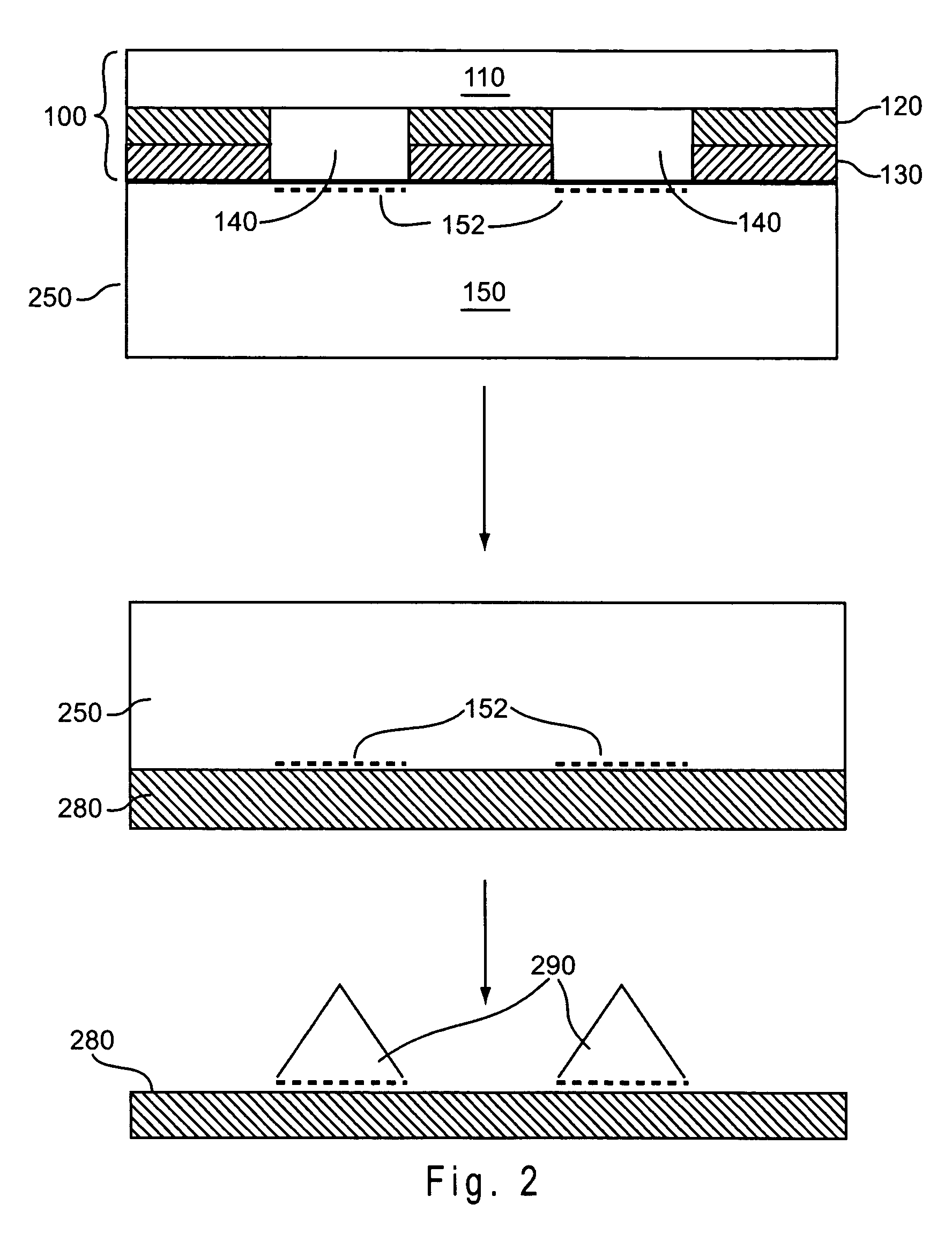
[0075]A PDMS stamp was formed as described in Example 2, except with an unbroken pattern of lines 2 μm wide and separated by 2 μm spacings. The stamp was placed into contact with the patterned side of the UVO photomask of Example 1 and irradiated through the mask for 4 minutes using a deuterium lamp. The mask was removed, and the PDMS pattern was placed into contact with a MPTMS silanized gold surface having a gold thickness of 100 nm and heated to 70° C. for 20 minutes. The PDMS stamp was then removed from the substrate using tweezers by peeling the stamp from a corner. FIGS. 6A and 6C are optical micrographs of the resulting microstructure, in which each circular domain (45×55 microns) on the gold surface contained a pattern of 2 μm wide lines of PDMS. The AFM line scan of FIG. 6B measured the height of the PDMS lines as approximately 1.6 μm.
[0076]The PDMS pattern was transferred into the gold film by wet etching the exposed gold layer and the underly...
PUM
| Property | Measurement | Unit |
|---|---|---|
| feature size | aaaaa | aaaaa |
| thickness | aaaaa | aaaaa |
| thickness | aaaaa | aaaaa |
Abstract
Description
Claims
Application Information