Ignoring switching transients, the ID·VDS product in the
power MOSFET remains small, and power dissipation in the switch remains low.
The process of removing charge stored in a
diode by reverse-biasing it immediately following forward conduction is referred to as forced
diode recovery, or “
reverse recovery.” In a
Schottky diode, however, since very few minority carriers are present during conduction, the
reverse recovery period can be very short or even negligible.
Some
ringing can lead to overshoot above the input voltage Vbatt as a result of
stray inductance in the circuit, particularly associated with
Schottky diode 7, and may inadvertently forward-bias the P-N junction in the normally off parasitic
diode 5.
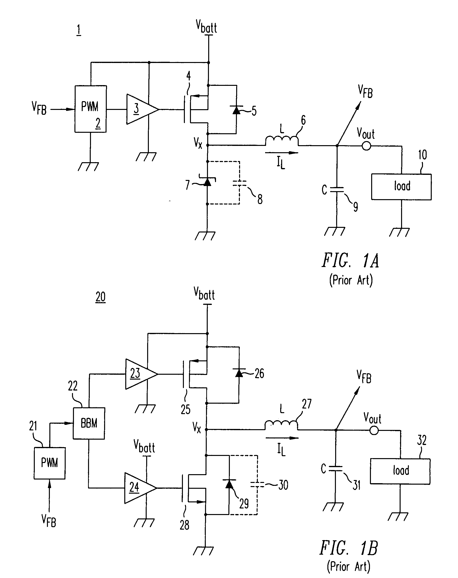
The addition of a
synchronous rectifier complicates the operation of a
Buck converter, since a break-before-make circuit is needed to guarantee that, during switching transitions, a brief moment exists when both MOSFETs are turned off, i.e. no current flows through either
MOSFET.
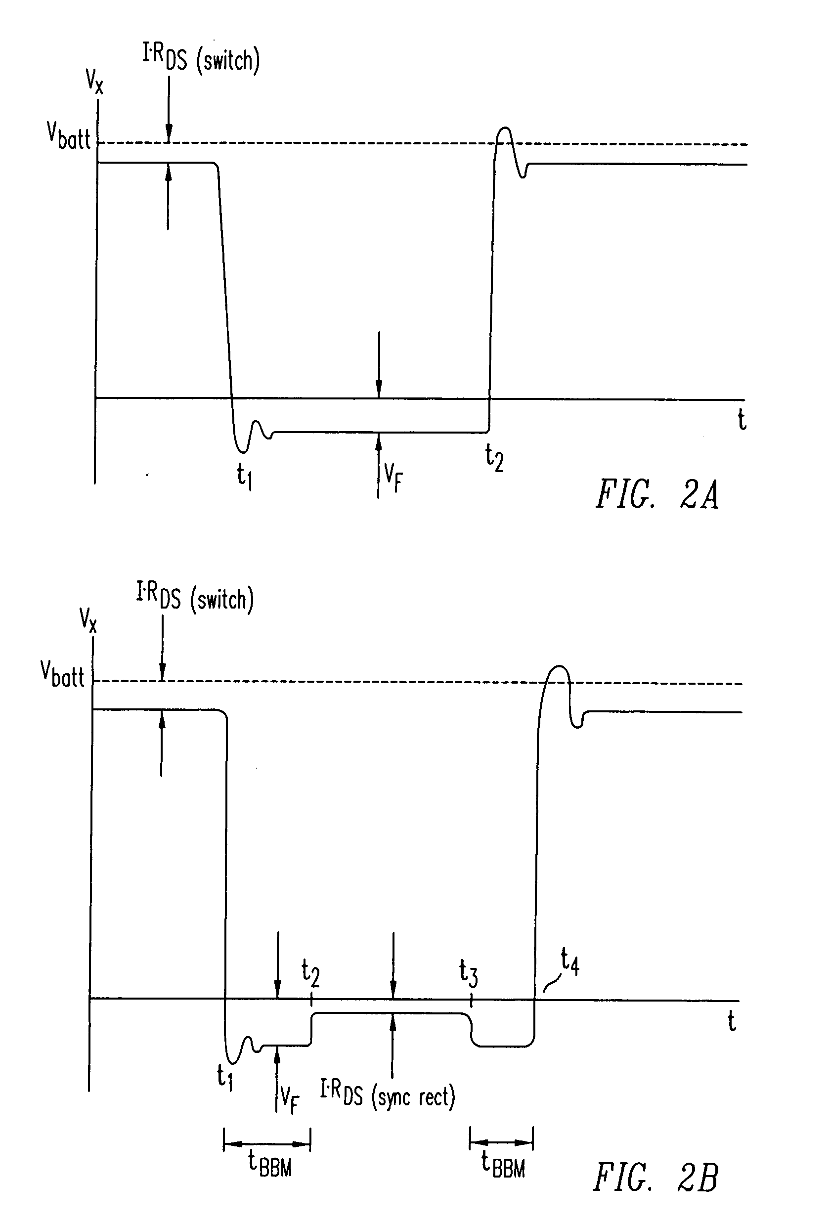
The BBM interval, while necessarily preventing
shoot through conduction, can lead to a variety of conditions giving rise to oscillations and electrical
noise.
Noisy operation may also arise when using a synchronous
rectifier under “
light load” conditions, when the load is drawing low current and the current in the
inductor can actually change direction temporarily.
Some overshoot and
ringing occurs due to stray inductances associated with the components' bond wires and
printed circuit board conductive traces.
This additional stored charge adversely impacts the switching transition at time t4, following the break-before-make interval.
In some instances the voltage Vx may “ring” above the input voltage Vbatt as a result of
stray inductance in the circuit, and lead to unwanted forward biasing of high-side diode 26, which in turn can lead to more charge storage, oscillations and circuit
instability.
This condition actually lowers the converter's efficiency for two reasons.
Unfortunately, diode 29 prevents the VDS from dropping until recovery is nearly complete.
First, both MOSFETs cannot operate as on-state switches at the same time without shorting out the power source input.
Diode conduction, however, leads to unwanted charge storage which not only can increase power losses but more importantly can result in increased noise, ringing, and
instability during switching events.
Attempts to divert the current from the
silicon diode using a discrete Schottky diode in parallel with the MOSFET offer limited benefits, especially since
stray inductance prevents the Schottky diode from conducting within the short BBM interval.
It should be noted, that transient simulations in commonly-used circuit simulators such as SPICE and its derivatives do not accurately predict diode recovery waveforms, since the compact
mathematical model for a P-N diode lacks the two-dimensional
physics describing
diffusion capacitance.
Another problem with the high dV / dt following diode recovery is MOSFET false turn-on induced noise.
The result is a burst of noise spread over a range of frequencies—noise especially problematic in communication applications.
In summary, forced diode recovery in a synchronous
Buck converter prior to high side conduction can lead to reverse
rectifier currents and efficiency loss, high dV / dt slew rates, ringing,
voltage overshoot, oscillations, forward-biasing of the high side MOSFET's diode, and uncontrollable bursts of noise spread across a range of frequencies.
Unfortunately, all known hard switching
converters, that is,
converters other than resonant and quasi-resonant converters, require forced diode recovery for some interval to extract charge stored in a P-N junction.
If a lower output current is required and the
clock period is not increased, the output voltage will start to rise and the converter will lose its ability to regulate.
The
disadvantage of PFM operation is that the variable frequency produces a varying
frequency noise spectrum, but efficiency remains relatively high.
Unfortunately, current reversal is energy inefficient,
wasting energy by “sloshing” current back and forth between the
inductor within the converter and the output
capacitor.
As a result, leaving the synchronous
rectifier MOSFET on during current reversal in
light load lowers the converter's efficiency.
In any case, large reverse-currents lower efficiency, and may potentially further aggravate noise during BBM operation and diode recovery.
Similar issues with uncontrolled charge storage in P-N diodes occur in synchronous boost converters.
As in a synchronous Buck converter, noisy forced-diode recovery in a synchronous
boost converter occurs due to unwanted diode conduction and charge storage during the break-before-make interval just prior to magnetizing the
inductor.
Like their synchronous Buck counterparts, synchronous boost converters also exhibit current reversal in
light load applications, leading to a loss of efficiency at low output currents, unless the synchronous rectifier MOSFET is turned off prior to current reversal.
Depending on when during or subsequent to oscillations 228 time t5 occurs, this transition may cause forced diode recovery, further exacerbating the noise problem.
In full-load operation, diode conduction in synchronous Buck and synchronous boost converters leads to unwanted charge storage, rapid transient behavior, and forced-diode-recovery-induced noise.
High slew rates also can result in false turn-on and by introducing substrate noise, provoke displacement-current-induced
CMOS latch-up.
CMOS latch-up is a potentially damaging condition wherein an
integrated circuit exhibits loss of control and high currents resulting from parasitic PNPN
thyristor conduction.
After the 2nd BBM interval 243, forced diode recovery 244 commences as the switch MOSFET temporarily becomes saturated, potentially generating substantial electrical noise.
In conclusion, uncontrolled diode conduction and charge storage occurring in synchronous Buck and synchronous boost converters during break-before-make operation and also during light-load conduction result in undesirable losses in efficiency, the generation of unwanted electrical and radiated noise, and numerous other potential issues such as false turn-on of an off-state MOSFET.
Problems with BBM operation, oscillations and poor efficiency during light load plague both synchronous boost and synchronous Buck converters.

