

Method for Manufacturing Semiconductor Device
a semiconductor and manufacturing technology, applied in the direction of vehicle route interaction devices, nuclear engineering, railway components, etc., can solve the problems of high cost of peeling resist mask effluent or disposal solution, difficult to apply laser ablation to a complicated stack structure, and high cost of etching gas disposal, etc., to achieve the effect of reducing cost, suppressing damage to the thin film and the base film of the thin film, and increasing throughpu
- Summary
- Abstract
- Description
- Claims
- Application Information
AI Technical Summary
Benefits of technology
Problems solved by technology
Method used
Image

Examples
embodiment modes
[0058] Embodiment Modes of the present invention, will now be described with reference to the drawings. Note that it is easily understood by those skilled in the art that the present invention can be carried out in many different modes, and various changes may be made in modes and details without departing from the spirit and the scope of the present invention. Therefore, the present invention should not be limited to the descriptions of the embodiment modes below. In addition, in the drawings, the same reference numerals are commonly given to the same components or components having the same function and the description therefor is not repeated.
embodiment mode 1
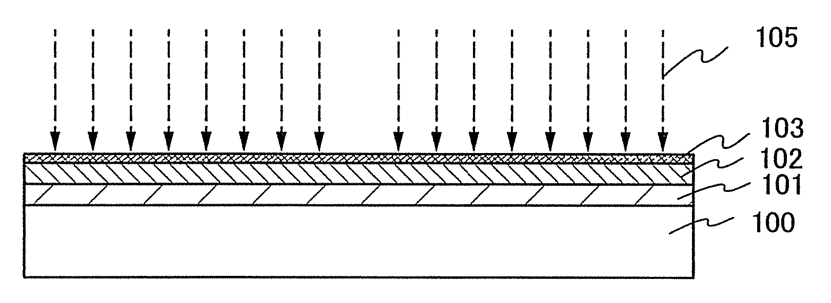
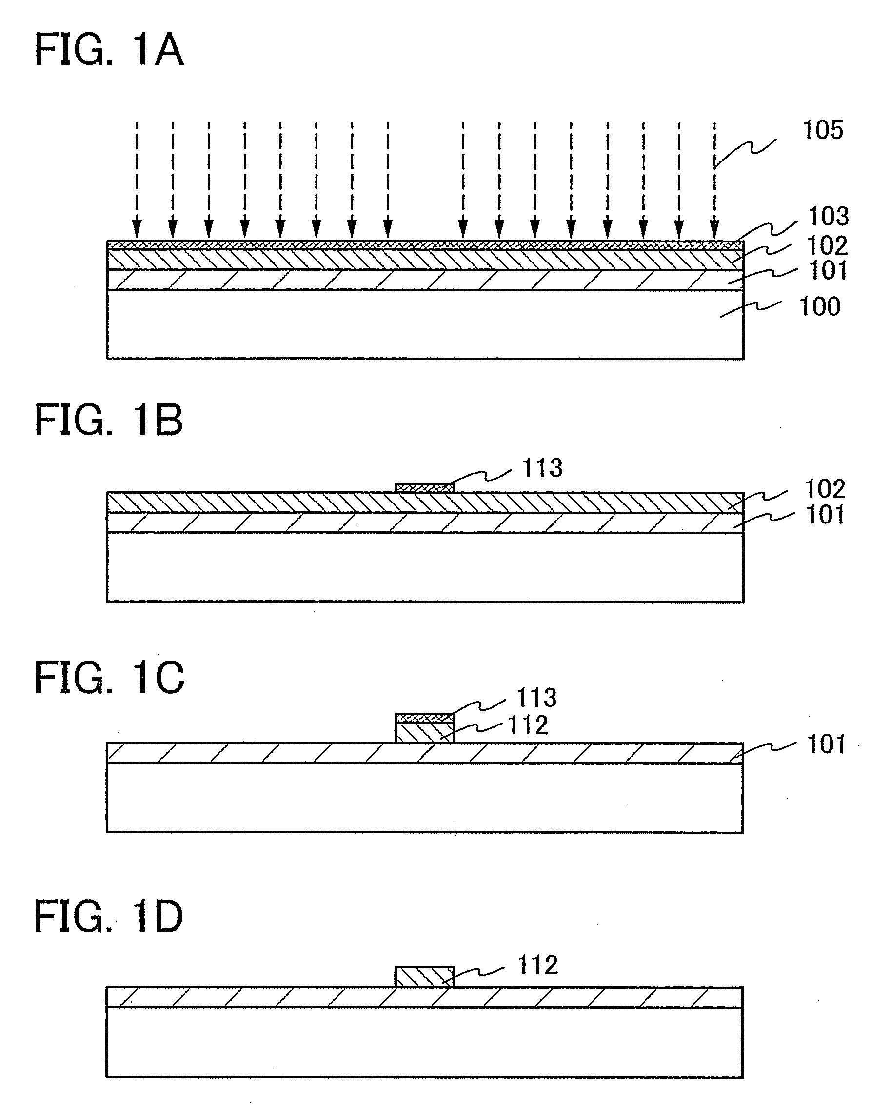
[0059] Embodiment Mode 1 will describe a thin film process using a laser beam, without a photolithography process. FIGS. 1A to 1D are cross-sectional views of a process for selectively forming a layer with a desired shape over a substrate.
[0060] As illustrated in FIG. 1A, a layer serving as a base film (hereinafter referred to as a base layer 101) is formed on one side of a substrate 100, a first layer 102 is formed over the base layer 101, and a peeling layer 103 is formed over the first layer 102.
[0061] As the substrate 100, a glass substrate, a plastic substrate, a metal substrate, a ceramic substrate, or the like can be used, as appropriate. Further, a printed wiring board or an FPC can be used. In a case where the substrate 100 is a glass substrate or a plastic substrate, a large-area substrate such as a substrate that is 320×400 mm, 370×470 mm, 550×650 mm, 600×720 mm, 680×880 mm, 1000×1200 mm, 1100×1250 mm, or 1150×1300 mm can be used. In this embodiment mode, a glass substr...
embodiment mode 2
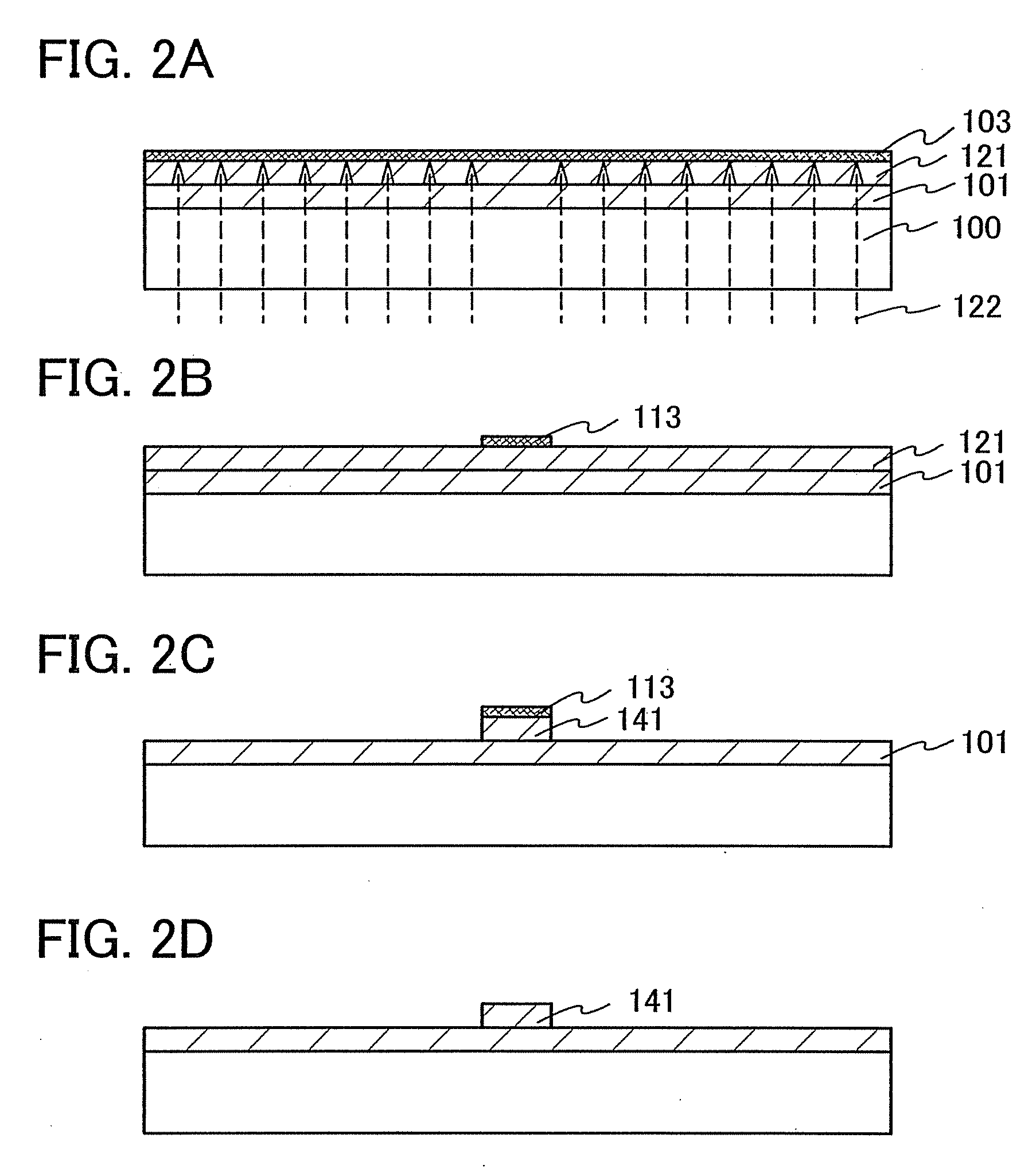
[0122] Embodiment Mode 2 will describe a process of forming a layer with a desired shape with reference to FIGS. 2A to 2D, which is different from Embodiment Mode 1. Embodiment Mode 2 is different from Embodiment Mode 1 in the direction of laser irradiation to a peeling layer.
[0123] As illustrated in FIG. 2A, similarly to Embodiment Mode 1, the base layer 101 is formed over the substrate 100, the first layer 121 is formed over the baser layer 101, and the peeling layer 103 is formed over the first layer 121.
[0124] In this embodiment mode, the substrate 100, the base layer 101 and the first layer 121 are preferably formed materials which can transmit a laser beam with which the peeling layer is irradiated later. In other words, materials having larger band gap than energy of a laser beam to be emitted are preferably used for formation of the layers. When a wavelength of the laser beam is in the visible region, a glass substrate, a quartz substrate, a plastic substrate which transmi...
PUM
| Property | Measurement | Unit |
|---|---|---|
| wavelength | aaaaa | aaaaa |
| thickness | aaaaa | aaaaa |
| thickness | aaaaa | aaaaa |
Abstract
Description
Claims
Application Information