Manufacture of electroless cobalt deposition compositions for microelectronics applications

a technology of electroless cobalt and composition, applied in the direction of liquid/solution decomposition chemical coating, solid/suspension decomposition chemical coating, coating, etc., can solve the problems of oxygen itself negatively affecting the deposit quality and device performance, prolonging shelf life, and improving the performance of solution

Inactive Publication Date: 2008-04-17
MACDERMID ENTHONE INC
View PDF17 Cites 10 Cited by
  • Summary
  • Abstract
  • Description
  • Claims
  • Application Information

AI Technical Summary

Benefits of technology

[0016]Among the various aspects of the invention may be noted the provision of a method for manufacturing an electroless cobalt deposition composition which enhances the performance of the solution by minimizing dissolved oxygen in the solution. Besides oxidizing Co2+ ions to Co3+ ions, oxygen itself negatively affects the deposit quality and device performance. An electroless cobalt deposition composition prepared according to this method is characterized by extended shelf life and improved plating performance. The improved plating composition results in defect-free or very low defectivity Co deposits for use as capping layers in microelectronic devices.

Problems solved by technology

Besides oxidizing Co2+ ions to Co3+ ions, oxygen itself negatively affects the deposit quality and device performance.

Method used


Image

  • Manufacture of electroless cobalt deposition compositions for microelectronics applications
  • Manufacture of electroless cobalt deposition compositions for microelectronics applications
  • Manufacture of electroless cobalt deposition compositions for microelectronics applications

Examples


example 1

Oxidation of Co(II) to Co(III) in Electroless Deposition Compositions with Solution Aging

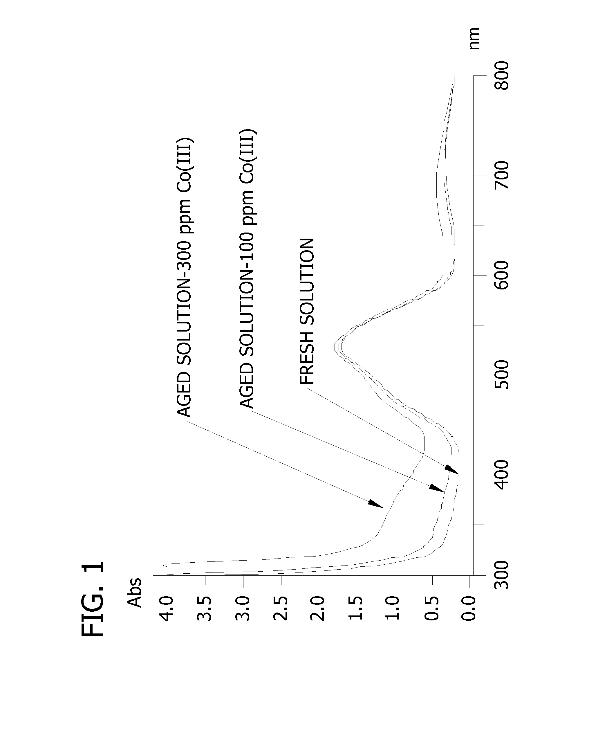
[0067]An electroless cobalt deposition composition was prepared, separated into samples, aged, and subjected to UV-Vis spectra analysis. See FIG. 1, which has wavelength (nm) on the x axis and absorbance on the y axis. The lower curve is analysis of a fresh solution; the middle curve is analysis of a solution aged for six months with limited air exposure. The upper curve is analysis of a solution aged for four months with extensive air and light exposure. These results show that absorbance in the range of 300 nm to 480 nm increases after the solutions were exposed to air and UV light for certain periods of time. Depending on exposure time and intensity, increases of the solution absorbance vary at wavelength shorter than 480 nm. The absorbance increase is believed mainly due to the formation of Co(III) species in the solutions. Similar absorbance changes were observed for the solutions spiked wi...

example 2

Determination of Induction Time for Electroless Deposition Compositions Comprising Known Concentrations of Co(III) Ion

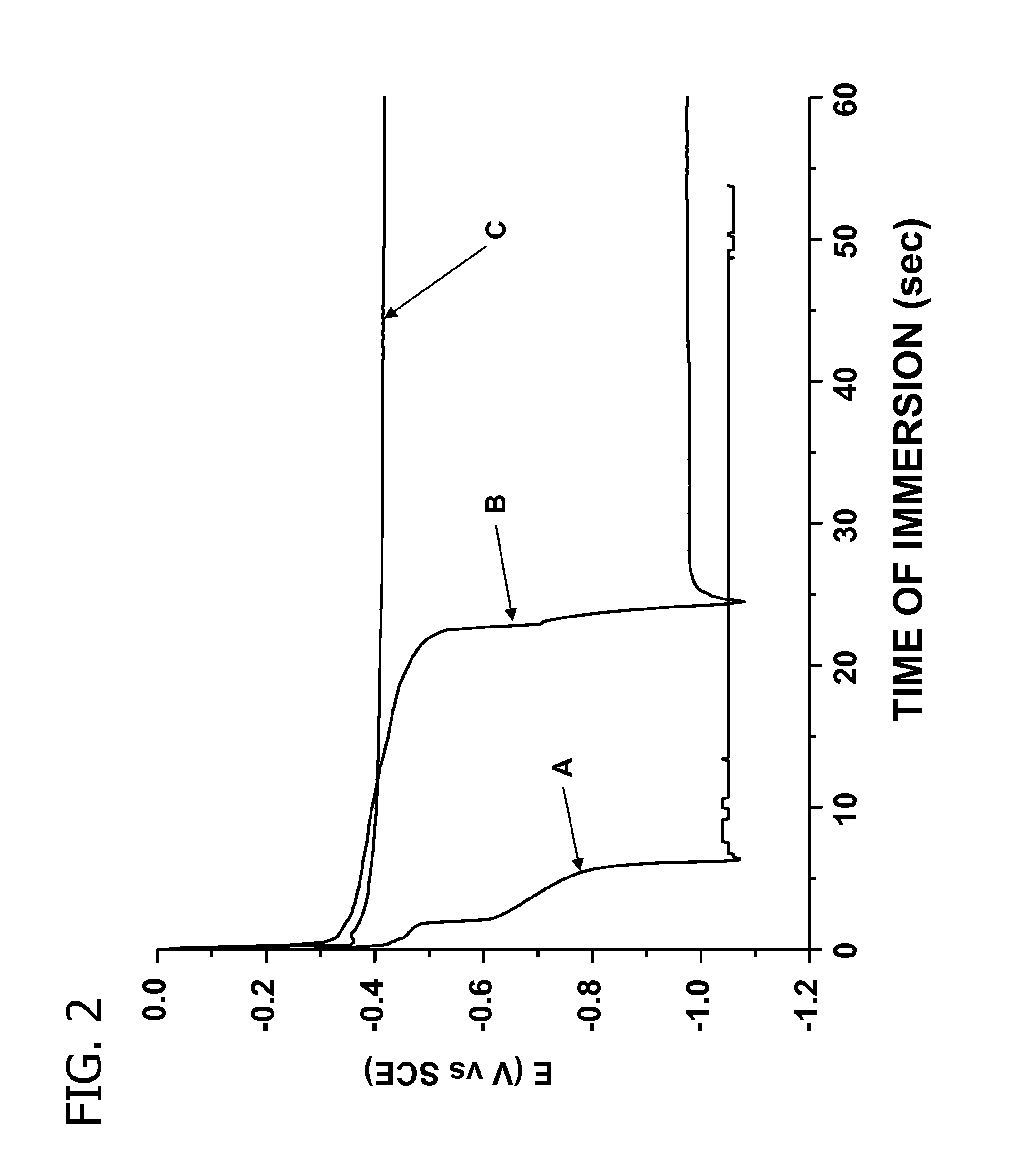
[0068]The induction times of fresh and aged electroless cobalt deposition compositions were measured. FIG. 2 is a graph depicting the induction times for the compositions: (A) freshly made solution having less than 0.1% oxidation, (B) aged solution having about 2% oxidation, and (C) aged solution having about 10% oxidation. It can be seen from the graph depicted in FIG. 2 that even a low extent of oxidation to Co(III) ion can lengthen Co deposition induction, and about 10% oxidation can prevent induction altogether for commercially practical purposes.

example 3

Determination of Deposition Height Variance for Electroless Deposition Compositions Comprising Known Concentrations of Co(III) Ion

[0069]Co(III) ions may affect the deposit thickness at different features of a patterned wafer substrate. To examine this phenomenon, two electroless cobalt deposition compositions were prepared having known Co(III) concentrations. Composition 1 is a Pd activated system while composition 2 is a self-initiated system. Samples of each composition, either as freshly prepared or aged for 6 months to allow cobalt oxidation to occur, were used to deposit cobalt alloy over dense and isolated features in a patterned wafer substrate. The deposit thicknesses over isolated and dense features from fresh and aged electroless cobalt deposition compositions are shown in the following Table I.

TABLE IThickness of Co DepositsComposition 1Composition 2Deposit thickness (Å)freshagedfreshagedDense features120 ± 10None105 ± 1685 ± 5Isolated features113 ± 16none100 ± 1466 ± 6Co...


PUM

PropertyMeasurementUnit
concentrationaaaaaaaaaa
temperatureaaaaaaaaaa
concentrationaaaaaaaaaa

Abstract

A method of preparing an aqueous electroless deposition composition for electrolessly depositing Co or a Co alloy onto a substrate in manufacture of microelectronic devices by treating water or an aqueous electroless deposition composition with a deoxygenating treatment to reduce the oxygen concentration.

Description

FIELD OF THE INVENTION[0001]This invention relates to electroless plating of Co and Co alloys in various plating industries, especially microelectronic device applications. More specifically, this invention relates to process control of solution manufacturing to yield an electroless Co plating composition exhibiting improved plating performance.BACKGROUND OF THE INVENTION[0002]Electroless deposition of Co is performed in a variety of applications in the manufacture of microelectronic devices. For example, Co is used in capping of damascene Cu metallization employed to form electrical interconnects in integrated circuit substrates. Copper can diffuse rapidly into a Si substrate and dielectric films such as, for example, SiO2 or low k dielectrics. Copper can also diffuse into a device layer built on top of a substrate in multilayer device applications. Such diffusion can be detrimental to the device because it can cause electrical leakage in substrates, or form an unintended electrica...

Claims


Application Information

Patent Timeline
Patent Type & Authority Applications(United States)
IPC IPC(8): H01L21/44C25D3/12
CPCC23C18/32H01L21/76849H01L21/288C23C18/50
Inventor CHEN, QINGYUNHURTUBISE, RICHARDPANECCASIO, VINCENTVALVERDE, CHARLESSTRITCH, DANIEL
Owner MACDERMID ENTHONE INC
Why Eureka
Try Eureka