Method for forming conductive layer and substrate having the same, and method for manufacturing semiconductor device
Inactive Publication Date: 2008-04-24
SEMICON ENERGY LAB CO LTD
View PDF11 Cites 15 Cited by
Summary
Abstract
Description
Claims
Application Information
AI Technical Summary
This helps you quickly interpret patents by identifying the three key elements:
Problems solved by technology
Method used
Benefits of technology
Benefits of technology
[0011] Based on the above, it is an object of the present invention to provide a method for forming conductive layers with little variation in resistance and flexible substrates having the conductive layers with a high yield. Further, it is also an object of the present invention to provide a method for manufacturing a semiconductor device that is small-sized, thin, and lightweight. Furthermore, it is another object of the present invention to provide a method for manufacturing a semiconductor device through less and safe steps.
[0022] The insulating layer that covers the conductive layer preferably serves as a protective film for preventing deterioration and oxidization of the conductive layer.
[0026] A layer in which oxygen and silicon are bonded and an inactive group is bonded to the silicon is easily divided by physical force; therefore, a conductive layer over the layer in which oxygen and silicon are bonded and an inactive group is bonded to the silicon can be separated from a substrate. Accordingly, the conductive layer that is formed over a substrate having heat resistance can be separated from the substrate, and the conductive layer can be easily formed.
[0027] Further, a flexible substrate having a conductive layer can be formed by attaching the conductive layer to a flexible substrate having low heat resistance. Therefore, conductive layers can be formed with a high yield, using a composition for which baking at a glass transition temperature of the flexible substrate or higher is necessary in a forming step. In a case where a composition that contains particles including a metal element is used, flexible substrates having conductive layers with little variation in resistance can be formed with a high yield.
[0028] By applying the composition to the depressed portion of the substrate, unevenness on a side surface of the printed composition can be reduced, and variation in shape and thickness can be reduced. Further, a width of the composition can be controlled, and thinning is possible. Furthermore, since the conductive layer can be formed without using a photolithography step, the number of processes and materials can be reduced, and therefore cost can be reduced.
[0029] By using such a conductive layer for an antenna, antennas with little variation in inductance can be formed. In addition, an antenna having high electromotive force can be formed. Further, by using such a layer for a wiring, a pixel electrode, or the like, semiconductor devices can be manufactured with a high yield. Furthermore, by using a flexible substrate having such a layer, formation of a semiconductor device that is small-sized, thin, and lightweight can be achieved. A semiconductor device can be manufactured through less and safe steps, and therefore cost of the semiconductor device can be reduced.
Problems solved by technology
Therefore, there is a problem in that a flexible substrate is deformed in a case of directly printing a composition that contains particles including a metal element over the flexible substrate and performing heating and baking to form a low-resistance conductive layer.
On the other hand, in a plating method, a baking step is not necessary, and a low-resistance conductive layer can be formed at a comparatively low temperature from approximately room temperature to 100° C. However, in a plating method, there are problems in that dangerous chemicals such as sulfuric acid, hydrochloric acid, and cyanogens compounds are used and waste fluids cause pollution.
Accordingly, in a case where a plurality of conductive layers is formed, there is variation in the thickness and shape of conductive layers, and as a result, there is a problem in that variation in resistance of the conductive layers occurs.
When an antenna, such as a wirelesschip capable of transmitting and receiving data wirelessly (also referred to as an ID tag, an IC tag, an IC chip, an RF (radio frequency) tag, a wireless tag, an electronic tag, or an RFID (radio frequencyidentification device)), is formed using such a conductive layer, inductance varies in a plurality of antennas, and a problem occurs in that variation in resonance frequency and electromotive force accompanying it occurs from one wirelesschip to another wireless chip.
Method used
Image
Click on the blue label to locate the original text in one second.
Reading with bidirectional positioning of images and text.
Examples
embodiment mode 1
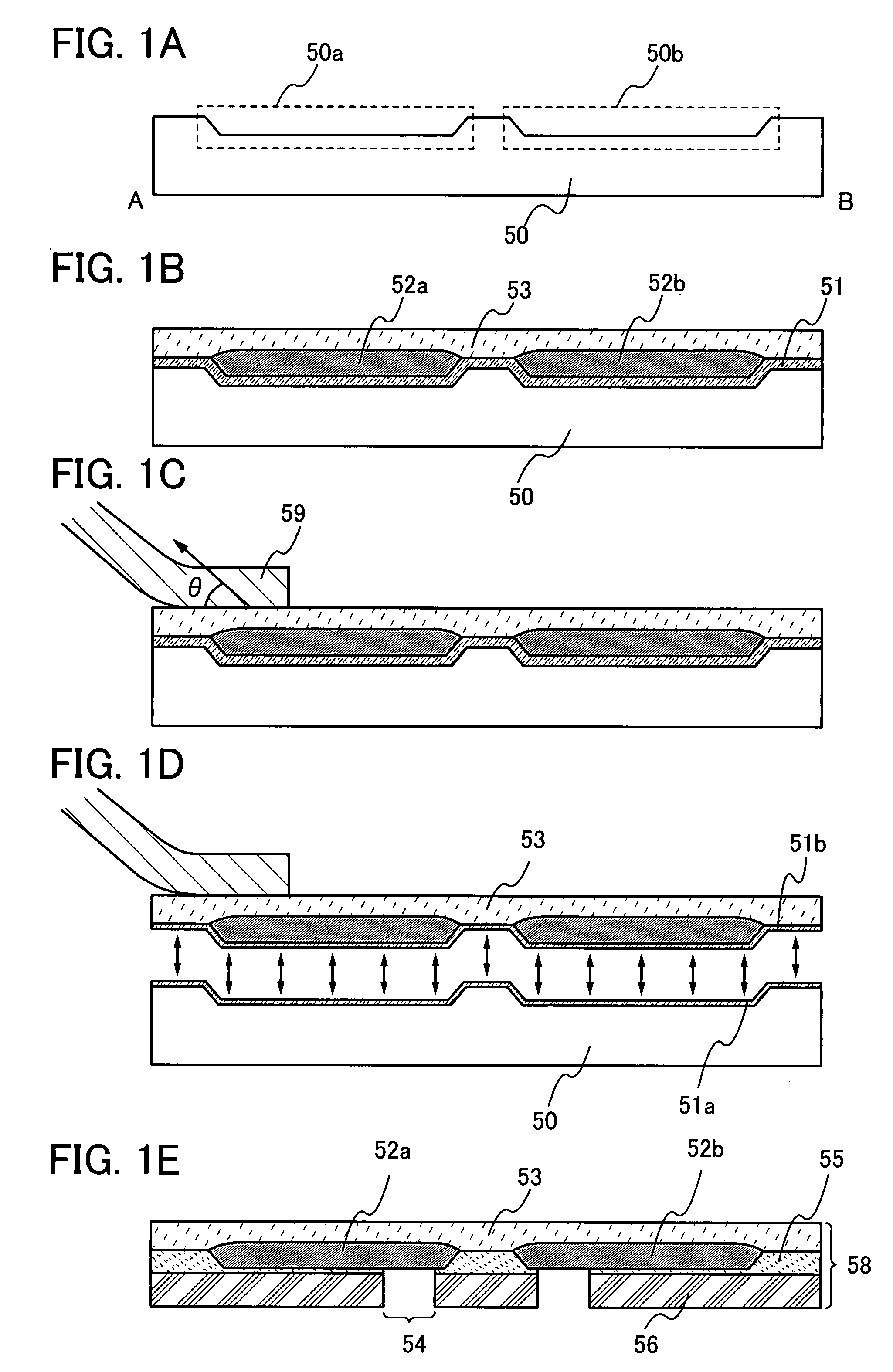
[0049] In this embodiment mode, one mode of a method for easily forming a conductive layer is described with reference to FIGS. 1A to 1E, FIG. 5, and FIGS. 12A and 12B. FIGS. 1A to 1E show cross-sectional views of a step of forming a conductive layer. FIG. 5 shows a top view of FIG. 1A. A cross-sectional view taken along a line A-B of FIG. 1A corresponds to a region A-B of a top view of FIG. 5. The conductive layer here serves as an antenna. In addition, a pixel electrode, a wiring, an electrode, and the like can be used as an application of a conductive layer, instead of an antenna.
[0050] As shown in FIG. 1A, a substrate 50 having depressed portions 50a and 50b is prepared.
[0051] As the substrate 50, a substrate having heat resistance against a baking temperature of conductive layers 52a and 52b is preferably used. Typically, a glass substrate, a quartz substrate, a ceramic substrate, a metal substrate, a silicon wafer, an organic resin layer, or the like can be used.
[0052] As t...
embodiment mode 2
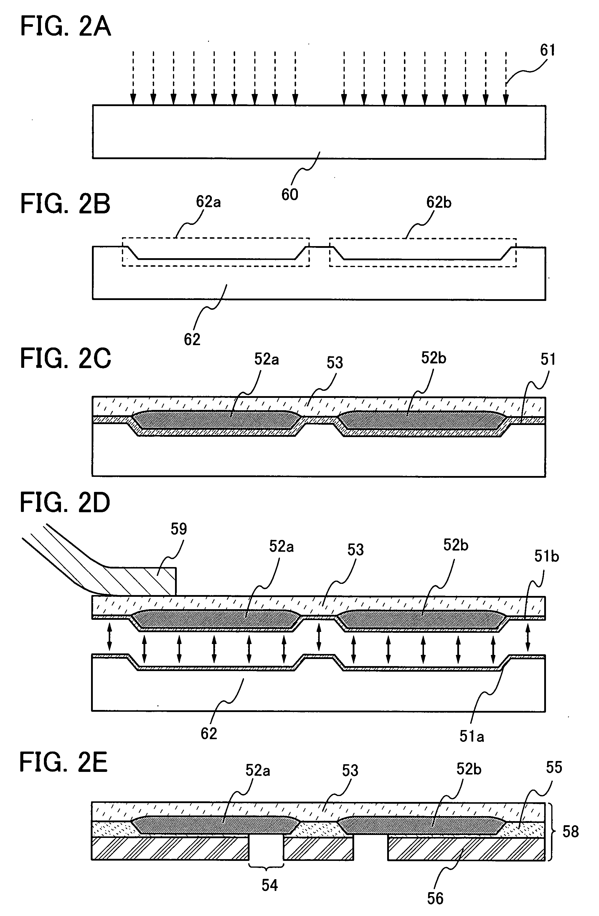
[0095] In this embodiment mode, one mode of a method for easily forming a conductive layer is described with reference to FIGS. 2A to 2E. FIGS. 2A to 2E show cross-sectional views of a step of forming a conductive layer.
[0096] As shown in FIG. 2A, a substrate 60 having a flat surface is prepared, and a surface of the substrate 60 is selectively treated, so that depressed portions 62a and 62b as shown in FIG. 2B are formed.
[0097] As the substrate 60, a substrate having heat resistance against a baking temperature of conductive layers 52a and 52b is preferably used. Typically, a glass substrate, a quartz substrate, a ceramic substrate, a metal substrate, a silicon wafer, an organic resin substrate, or the like can be used.
[0098] As treatment by which the depressed portions 62a and 62b are formed in the substrate, laserlight irradiation, cutting, etching of a substrate using a resistmask formed in a photolithography step, or the like can be given. In a case where the substrate is ...
embodiment mode 3
[0104] In this embodiment mode, a method for forming a conductive layer that can reduce variation in resistance in different conductive layers is described with reference to FIGS. 3A to 3D. Here, Embodiment Mode 1 is used for the description; however, Embodiment Mode 2 can also be applied.
[0105] As shown in FIG. 3A, in the same manner as in Embodiment Mode 1, over a substrate 50 having depressed portions, a layer 51 in which oxygen and silicon are bonded and an inactive group is bonded to the silicon is formed using a silanecoupling agent. Compositions 70a and 70b are applied in depressed portions 50a and 50b over the layer 51 in which oxygen and silicon are bonded and an inactive group is bonded to the silicon.
[0106] Next, portions of the compositions that are higher than a surface of the layer 51 in which oxygen and silicon are bonded and an inactive group is bonded to the silicon are removed to flatten a surface. Alternatively, a region in the compositions 70a and 70b where a ...
PUM
Abstract
A separation layer is formed over a substrate having a depressed portion, using a silanecoupling agent; a conductive layer and an insulating layer that covers the conductive layer are formed in the depressed portion over the separation layer; and a sticky member is attached to the insulating layer, then the conductive layer and the insulating layer are separated from the substrate. Alternatively, after these steps, a flexible substrate is attached to the conductive layer and the insulating layer.
Description
BACKGROUND OF THE INVENTION [0001] 1. Field of the Invention [0002] The present invention relates to a method for forming a conductive layer and a substrate having the conductive layer. Further, the present invention also relates to a method for manufacturing a semiconductor device having a conductive layer. [0003] 2. Description of the Related Art [0004] Conventional methods for forming a conductive layer serving as an antenna, a pixel electrode, a wiring, or the like over a flexible substrate include the following: a method in which a composition that contains particles including a metal element is printed over a flexible substrate by a screen printing method and the composition is then heated and baked to form a conductive layer; and a method in which a conductive layer is formed over a flexible substrate by a plating method. [0005] Patent Document 1: Japanese Published Patent Application No. 2004-310502 [0006] In order to form a low-resistance conductive layer by using a composi...
Claims
Application Information
Patent Timeline
Application Date:The date an application was filed.
Publication Date:The date a patent or application was officially published.
First Publication Date:The earliest publication date of a patent with the same application number.
Issue Date:Publication date of the patent grant document.
PCT Entry Date:The Entry date of PCT National Phase.
Estimated Expiry Date:The statutory expiry date of a patent right according to the Patent Law, and it is the longest term of protection that the patent right can achieve without the termination of the patent right due to other reasons(Term extension factor has been taken into account ).
Invalid Date:Actual expiry date is based on effective date or publication date of legal transaction data of invalid patent.

