Multi image storage on sensor

a sensor and image technology, applied in the field of cmos image sensors, can solve the problems of readout noise and non-uniformity, image sensor devices such as ccds that integrate charge created by incident photons, and limited dynamic range, so as to improve sensitivity, eliminate motion blur, and extend the dynamic range and autofocus

Inactive Publication Date: 2008-05-08
EASTMAN KODAK CO
View PDF4 Cites 35 Cited by
  • Summary
  • Abstract
  • Description
  • Claims
  • Application Information

AI Technical Summary

Benefits of technology

[0020]The present invention includes the advantages of digital image stabilization, increased sensitivity, elimination of motion blur, extended dynamic range and autofocus.

Problems solved by technology

Image sensor devices, such as a CCD that integrate charge created by incident photons, have dynamic range limited by the maximum amount of charge that can be collected and held in a given photodetector.
A drawback, however, is that CMOS image sensors generally include lower DR and higher SNL than CCDs due to their high readout noise and non-uniformity.
The same limitations on DR exist for CMOS devices as on CCDs.
Vsat is limited by the amount of charge that can be held and isolated in the photodetector and excess charge is lost.
This can become even more problematic with CMOS compared to CCD due to additional circuitry in the form of active components such as analog-to-digital converters, timing circuits and other custom circuitry such as “system on a chip” that are associated with the photodetector that further limits the area available for the photodetector.
CMOS devices also use a low voltage supply which increases the impact of thermally created noise.
In addition, the active components on CMOS devices, that are not present on CCDs, provide a much higher noise floor on CMOS devices compared to CCDs.
This is due to higher temporal noise as well as possibly quantization noise from the on-chip analog-to-digital converter.
However, creating a multiple exposure photograph with a digital camera by repeatedly exposing the sensor to light is problematic, due to noise buildup on the sensor.
This approach does have limitations in that the image processing is typically done on rendered images which have been color corrected and compressed which when added together can produce artifacts.
A more complicated use of the multiple exposure technique is when images are combined to increase depth of field.
In this case, the photographer wishes to keep the aperture at minimal size to provide a large depth of field but the flash equipment is not powerful enough to provide correct exposure with the small aperture.
It is possible in this case to increase the exposure time and to program the flash to fire several times. However, the combination of the increased exposure time and the time required for the flash to recharge between firing increases the time for thermally generated noise to build up on the image sensor resulting in a noisy image.
However, in the digital case, combining such differently lit images using image-processing software after they have been captured digitally and rendered, cannot be done in a linear fashion for the reasons mentioned above.
Likewise, adding the images directly on the sensor is not possible due to noise considerations, as mentioned above.
In high contrast scenes, the dynamic range of the camera sensor is often not adequate to provide detail for both dark and light portions of the image, for images captured on CCDs or CMOS devices.

Method used


Image

  • Multi image storage on sensor
  • Multi image storage on sensor
  • Multi image storage on sensor

Examples


Embodiment Construction

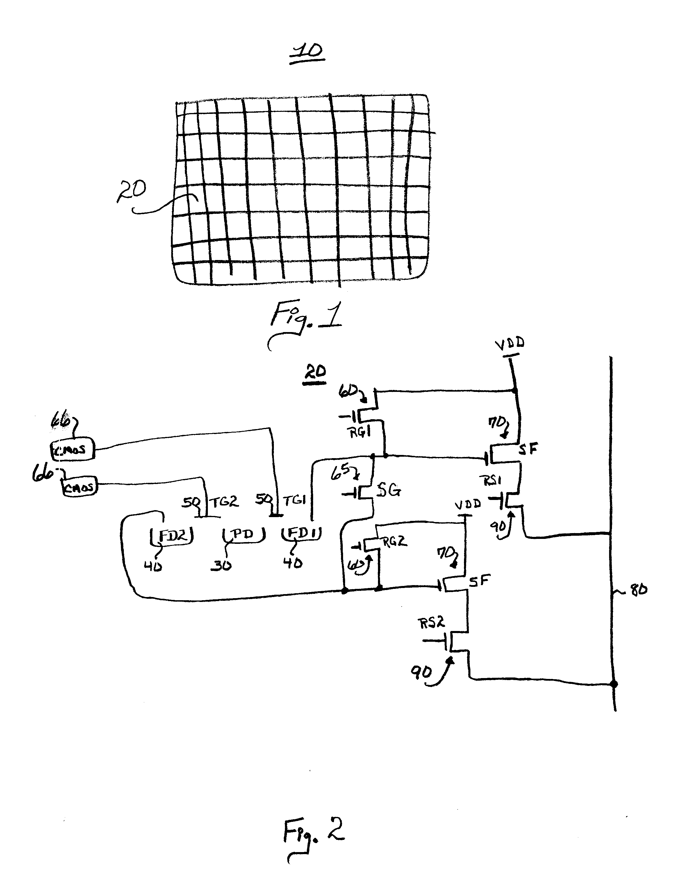
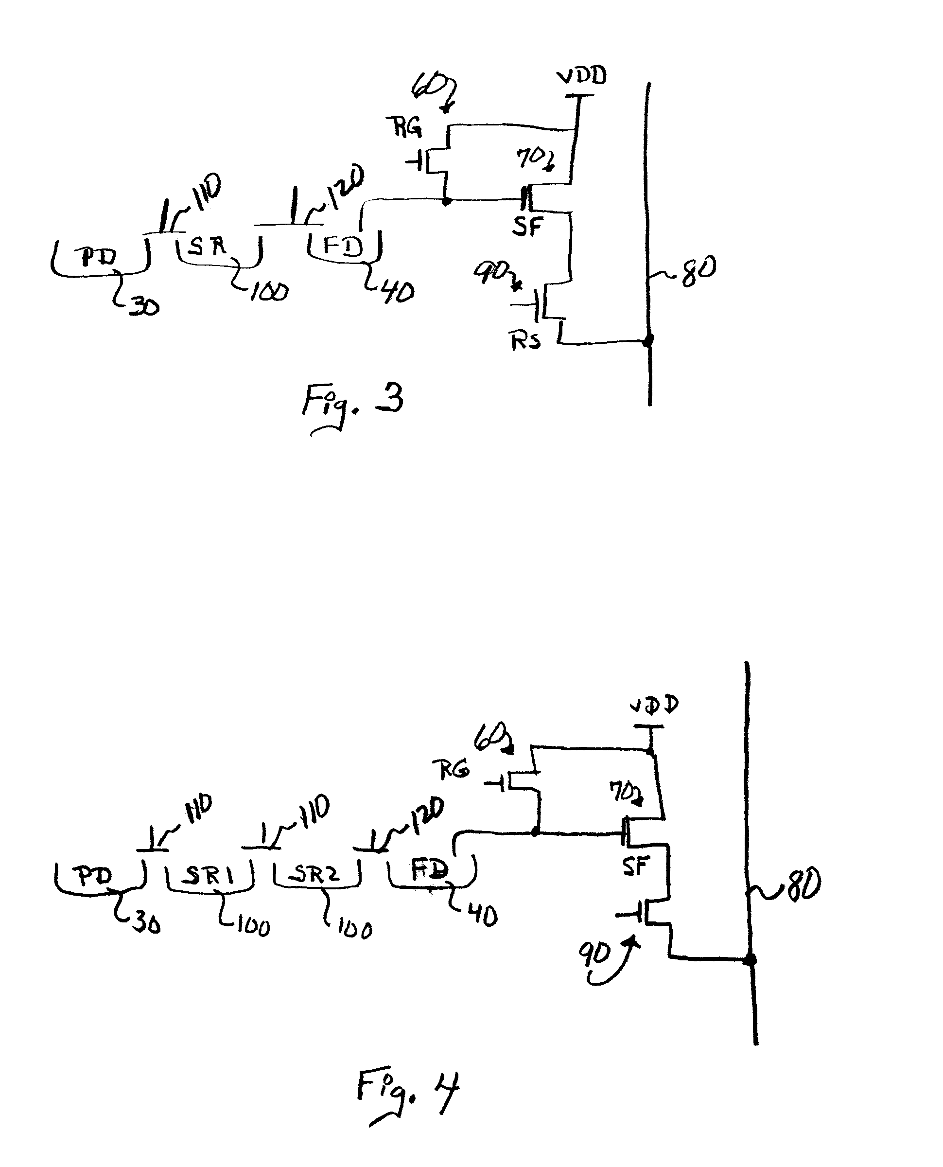
[0028]Before discussing the present invention in detail, it is instructive to note that the present invention is preferably used in, but not limited to, a CMOS active pixel sensor. Active pixel sensor refers to an active electrical element within the pixel, more specifically an amplifier. CMOS refers to complementary metal oxide silicon type electrical components such as transistors which are associated with the pixel, but typically not in the pixel, and which are formed when the source / drain of a transistor is of one dopant type and its mated transistor is of the opposite dopant type. CMOS devices include advantages on of which is they consume less power.

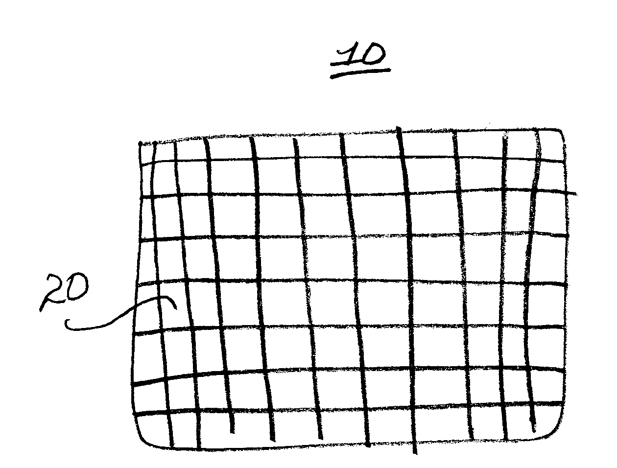
[0029]Referring to FIG. 1, there is shown an image sensor 10 of the present invention having a plurality of pixels 20 arranged in a two-dimensional array. Although a two-dimensional array is shown as a preferred embodiment, the present invention is not limited to a two-dimensional array; as is apparent to those skilled in the art, ...


PUM


Abstract

An image sensor includes a plurality of pixels with each pixel having a photosensitive area that captures a sequence of at least two light exposures by accumulating photon-induced charge for each exposure; at least two charge storage areas each of which is associated respectively with one of the sequence of light exposures into which the accumulated charge for each exposure is transferred sequentially; and at least one amplifier that is associated with at least one of the charge storage areas.

Description

FIELD OF THE INVENTION[0001]The invention relates generally to the field of CMOS image sensors and, more particularly, to such sensors that capture a sequence of images respectively in two or more floating diffusions.BACKGROUND OF THE INVENTION[0002]Solid-state image sensors are now used extensively in many types of image capture applications. The two primary image sensor technologies utilized are Charge Coupled Devices (CCD) and complimentary metal oxide semiconductor (CMOS) devices. Both are basically a set or array of photodetectors that convert incident light into an electrical signal that can be readout and used to construct an image correlated to the incident light pattern. The exposure or integration time for the array of photodetectors can be controlled by well-known mechanisms such as a mechanical shutter or an electrical shutter. The electrical signal represents the amount of light incident upon the individual photodetectors in the array of photodetectors on the image sens...

Claims


Application Information

Patent Timeline
Patent Type & Authority Applications(United States)
IPC IPC(8): H04N5/335
CPCH04N5/35572H04N5/35581H04N5/37452H04N5/3745H04N5/3559H04N25/587H04N25/589H04N25/59H04N25/77H04N25/771H04N25/62H04N25/76
Inventor BORDER, JOHN N.HAMILTON, JOHN F.COMPTON, JOHN T.
Owner EASTMAN KODAK CO
Why Eureka
Try Eureka