Semiconductor device and method of forming the same

a technology of semiconductors and devices, applied in the direction of semiconductor devices, electrical devices, transistors, etc., can solve the problems of reducing the capacity of capacitors, inhibiting the high performance of drams, etc., to prevent the abnormality of silicidation reactions, reduce contact resistance, and large contact area

Active Publication Date: 2008-05-29
MICRON TECH INC
View PDF2 Cites 36 Cited by
  • Summary
  • Abstract
  • Description
  • Claims
  • Application Information

AI Technical Summary

Benefits of technology

[0026]It is another object of the present invention to provide a semiconductor device including a capacitor that has a bottom electrode of a metal or a metallic compound which is connected to a capacitor contact plug such that it is easy both to prevent the abnormality of silicidation reaction on the interface between the capacitor contact plug and the bottom electrode of the capacitor and to ensure a sufficiently large contact area between them and reduce the contact resistance between them, while keeping a high yield of manufacturing the semiconductor device.
[0028]It is a still further object of the present invention to provide a method of forming a semiconductor device including a capacitor that has a bottom electrode of a metal or a metallic compound which is connected to a capacitor contact plug such that it is easy both to prevent the abnormality of silicidation reaction on the interface between the capacitor contact plug and the bottom electrode of the capacitor and to ensure a sufficiently large contact area between them and reduce the contact resistance between them, while keeping a high yield of manufacturing the semiconductor device.

Problems solved by technology

The limited plan-area for the capacitor may result in reduced capacity of the capacitor.
The reduction in the capacity of the capacitor may make it difficult for the conventional DRAM to ensure the normal memory operation thereof There was an issue of how to ensure the necessary capacity of the capacitor of each memory cell when each memory cell is shrunken.
Increasing the contact resistance may inhibit desired high performance of the DRAM.
When the capacitor holes 101 have a high aspect ratio or a greater depth, an insufficient amount of titanium may be supplied on the surface of each silicon contact pad, thereby causing an abnormal silicidation reaction.
As a result, a desired or intended silicide layer can not be formed.
High aspect ratio or larger depth of the capacitor holes may cause insufficient amount of titanium to be supplied on the bottoms of the capacitor holes, thereby forming undesired or unintended silicide layers of off-stoichiometric composition on the surfaces of the silicon contact pads.
Further, silicon migration can be caused, thereby forming voids on the surfaces of the silicon contact pads.
Such voids may cause bad connection between the bottom electrode 106 and the silicon contact pads.
When the bottom electrode is made of a metal or a metal compound, the abnormal silicidation reaction can be caused thereby making it difficult to ensure the electronic connection between the capacitor contact plug and the bottom electrode of the capacitor.
This structure may, however, not prevent the other problem with misalignment between the capacitor contact plug and the capacitor hole.
As described above, the misalignment decreases the contact area between the capacitor contact plug and the bottom electrode of the capacitor, thereby making it difficult to ensure the minimum necessary contact area for obtaining sufficiently reduced contact resistance between the capacitor contact plug and the bottom electrode of the capacitor.
In accordance with the conventional method of forming a capacitor having a bottom electrode of a metal or a metallic compound which is connected to a capacitor contact plug, it is not easy both to prevent the abnormality of silicidation reaction on the interface between the capacitor contact plug and the bottom electrode of the capacitor and to ensure a sufficiently large contact area between them and reduce the contact resistance between them.
This results in decreasing the yield of manufacturing the semiconductor device.

Method used


Image

  • Semiconductor device and method of forming the same
  • Semiconductor device and method of forming the same
  • Semiconductor device and method of forming the same

Examples


first embodiment

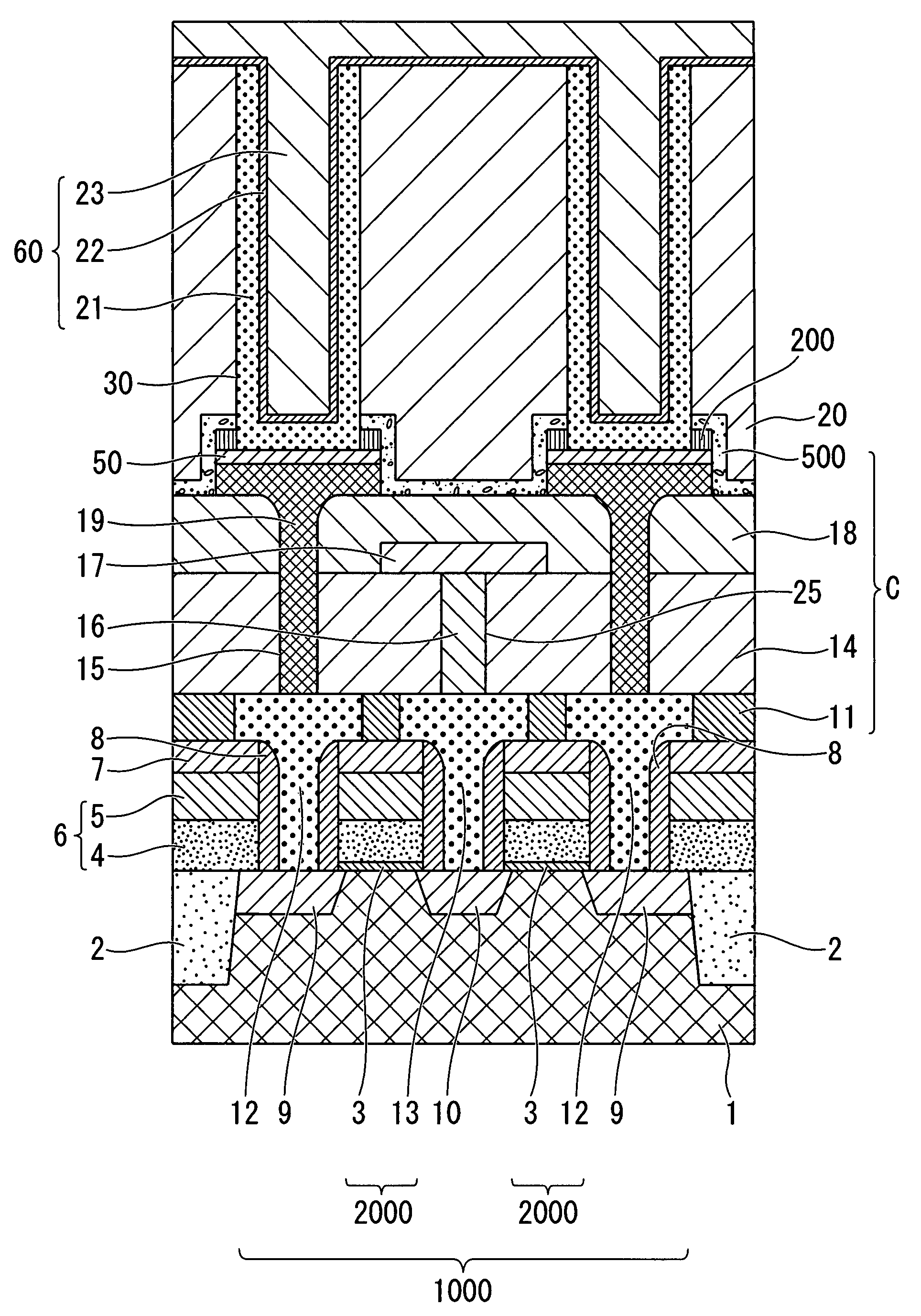
[0057]A semiconductor device such as a DRAM of this first embodiment will be described with reference to the drawings. FIG. 1 is a fragmentary cross sectional elevation view illustrating a semiconductor device in accordance with a first embodiment of the present invention.

[0058]A semiconductor substrate 1 is made of a semiconductor such as silicon doped with a p-type impurity such as boron.

[0059]A device isolation region 2 is selectively provided in the semiconductor substrate 1. The device isolation region 2 defines or surrounds an active region so called to as a transistor formation region for forming a transistor that selects a memory cell. The device isolation region 2 can be formed by a shallow trench isolation method.

[0060]In the transistor formation region, gate insulating films 3 are provided over the surface of the semiconductor substrate 1. The gate insulating films 3 may be made of silicon oxide. In this case, the gate oxide films 3 can be formed by a thermal oxidation me...

second embodiment

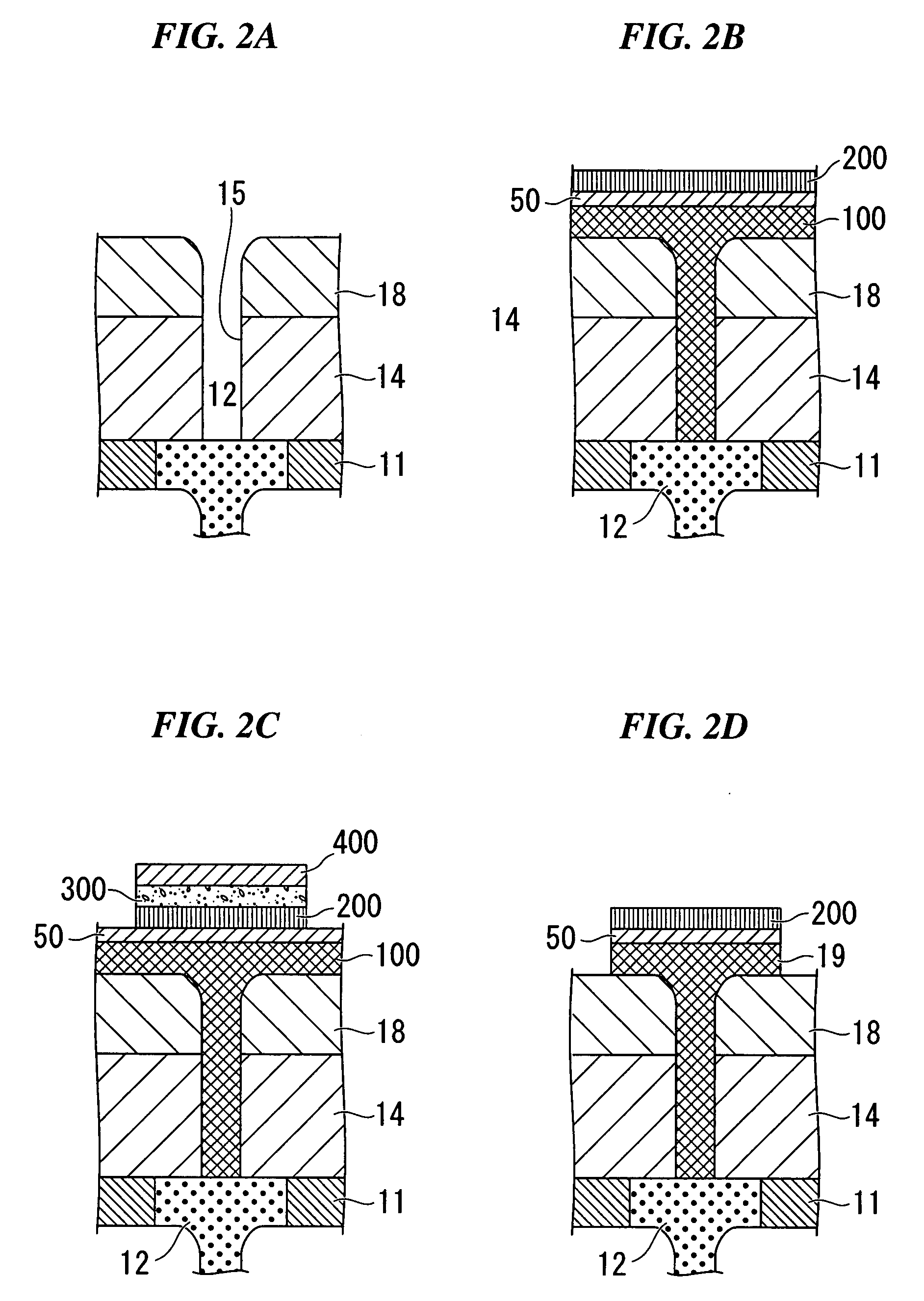
[0122]A semiconductor device such as a DRAM of this second embodiment will be described with reference to the drawings. The second embodiment is different from the first embodiment in the shape of the capacitor contact plug and the fabrication process for the contact plug. The following descriptions will focus on the differences of the second embodiment from the first embodiment. FIGS. 4A through 4D are fragmentary cross sectional elevation views illustrating capacitor contact plugs, in sequential steps involved in a method of forming the DRAM memory cell of the second embodiment.

[0123]Processes resulting in forming the bit line layer 17 are carried out in the same ways as described in the first embodiment. Duplicate descriptions of the same processes will be omitted.

[0124]A plasma enhanced chemical vapor deposition process is carried out to form an inter-layer insulator 18 of silicon oxide over the bit line layer 17 and the inter-layer insulator 14. The inter-layer insulator 18 has...


PUM


Abstract

A semiconductor device may include a MOS transistor having source and drain regions in a semiconductor substrate, a first inter-layer insulator having first contact holes that reach the source and drain regions over the MOS transistor. Cell contact plugs in the first contact holes contact with the source and drain regions. A second inter-layer insulator over the first inter-layer insulator and the cell contact plugs has second contact holes that reach the cell contact plugs. Contact plugs each have first and second portions. The first portion is in the second contact hole. The second portion extends over the first second inter-layer insulator. Metal barrier layers cover the upper surfaces of the second portions of the contact plugs. Capacitors each have a bottom electrode layer, a capacitive insulating layer and a top electrode layer. The bottom electrode layers each have a contact portion that contacts with the metal barrier layer.

Description

BACKGROUND OF THE INVENTION[0001]1. Field of the Invention[0002]The present invention generally relates to a semiconductor device and a method of forming the same. More specifically, the present invention relates to a semiconductor memory device such as DRAM (Dynamic Random Access Memory) including memory cells having contact structures and a method of forming the same.[0003]Priority is claimed on Japanese Patent Application No. 2006-317302, filed Nov. 24, 2006, the content of which is incorporated herein by reference.[0004]2. Description of the Related Art[0005]All patents, patent applications, patent publications, scientific articles, and the like, which will hereinafter be cited or identified in the present application, will hereby be incorporated by reference in their entirety in order to describe more fully the state of the art to which the present invention pertains.[0006]The DRAM has memory cells, each of which may have a pair of a single transistor for selecting a memory cel...

Claims


Application Information

Patent Timeline
Patent Type & Authority Applications(United States)
IPC IPC(8): H01L29/94H01L21/8242
CPCH01L21/7685H01L21/76852H01L27/10855H01L21/76889H01L27/10814H01L21/7687H10B12/315H10B12/0335
Inventor OHUCHI, MASAHIKO
Owner MICRON TECH INC
Why Eureka
Try Eureka