Method for fabricating semiconductor device

a semiconductor and device technology, applied in the direction of semiconductor devices, basic electric elements, electrical equipment, etc., can solve the problems of junction leakage and low and achieve the effect of improving thermal stability of nickel silicid

Inactive Publication Date: 2008-05-29
FUJITSU SEMICON LTD
View PDF16 Cites 40 Cited by
  • Summary
  • Abstract
  • Description
  • Claims
  • Application Information

AI Technical Summary

Benefits of technology

[0013]The present invention was made under the background circumstances described above. An object of the present invention

Problems solved by technology

However, the thermal stability of nickel silicide is low, so nickel silicide easily agglomerates at a temperature

Method used


Image

  • Method for fabricating semiconductor device
  • Method for fabricating semiconductor device
  • Method for fabricating semiconductor device

Examples


Embodiment Construction

[0031]Embodiments of the present invention will now be described in detail with reference to the drawings.

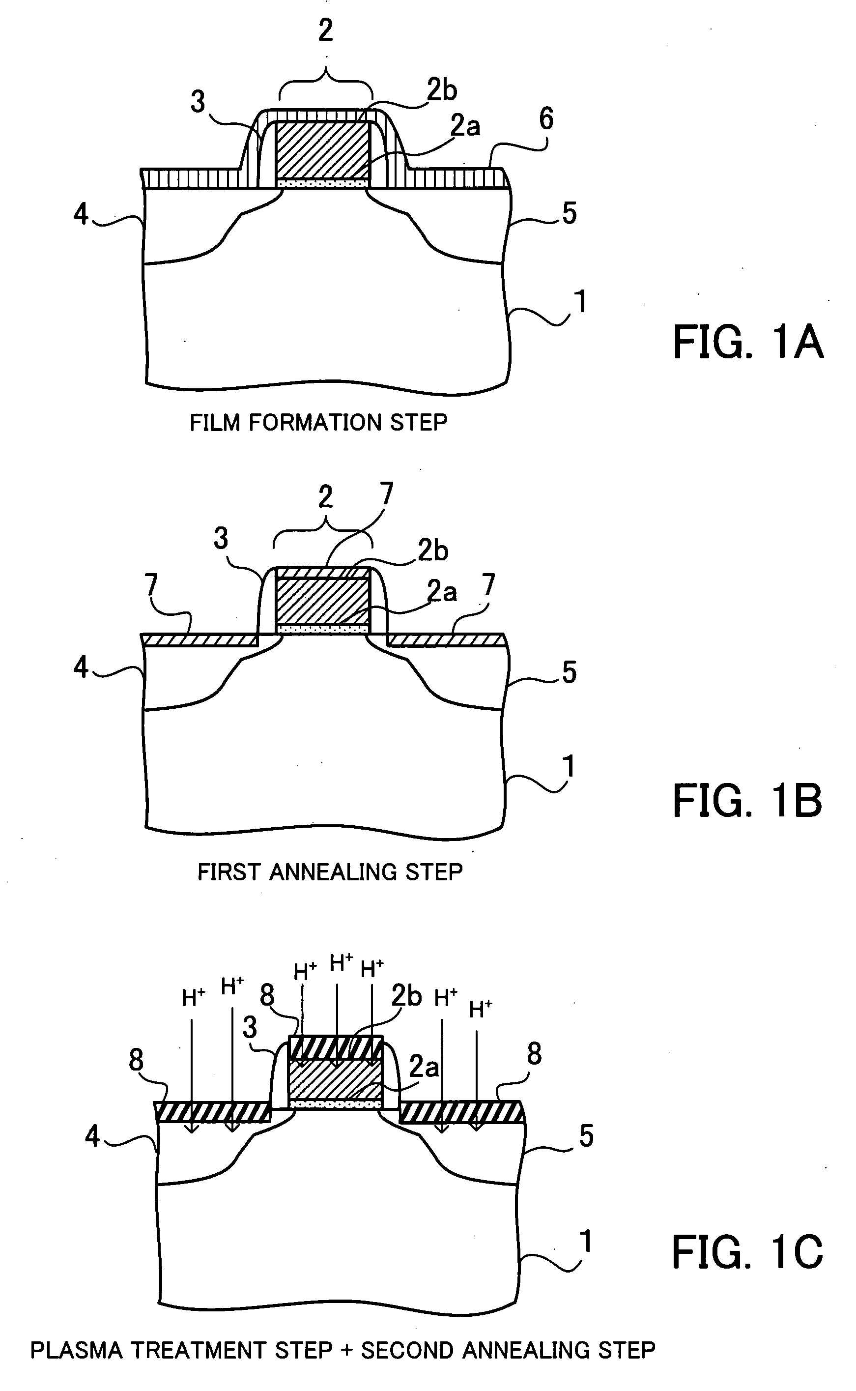
[0032]FIGS. 1A, 1B, and 1C are schematic sectional views showing a method for fabricating a semiconductor device, according to an embodiment of the present invention.

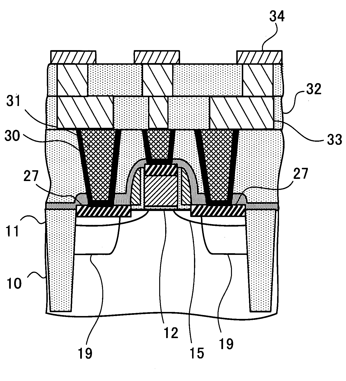
[0033]It is assumed that a gate region 2, a sidewall 3, a source region 4, and a drain region 5 are formed on a semiconductor substrate 1 which is, for example, a (100) silicon substrate by known fabrication steps. The gate region 2 includes a gate insulating film 2a and a polycrystalline silicon gate 2b formed over the gate insulating film 2a. A nickel film 6 is formed over the semiconductor substrate 1 (film formation step (FIG. 1A)).

[0034]A nickel alloy film which contains one or more of platinum, tungsten, tantalum, and palladium may be formed in place of the nickel film 6.

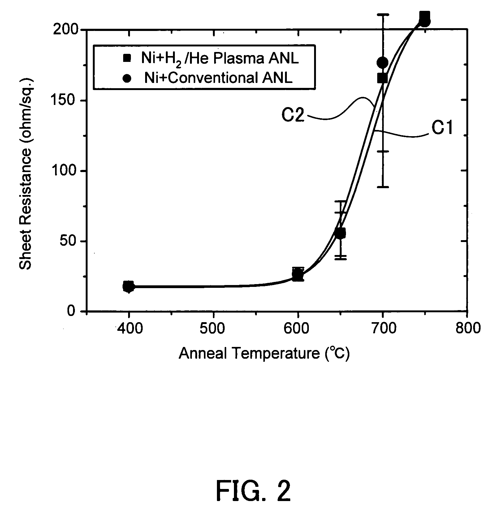
[0035]Annealing treatment is then performed in an atmosphere of an inert gas, such as N2 or argon (Ar), at a temperature of about 260° C. to ...


PUM


Abstract

A semiconductor device fabrication method by which the thermal stability of nickel silicide can be improved. Nickel (or a nickel alloy) is formed over a semiconductor substrate on which a gate region, a source region, and a drain region are formed. Dinickel silicide is formed by performing a first annealing step, followed by a selective etching step. By performing a plasma treatment step, plasma which contains hydrogen ions is generated and the hydrogen ions are implanted in the dinickel silicide or the gate region, the source region, and the drain region under the dinickel silicide. The dinickel silicide is phase-transformed into nickel silicide by performing a second annealing step.

Description

CROSS-REFERENCE TO RELATED APPLICATIONS[0001]This application is based upon and claims the benefits of priority from the prior Japanese Patent Application No. 2006-321742, filed on Nov. 29, 2006, the entire contents of which are incorporated herein by reference.BACKGROUND OF THE INVENTION[0002](1) Field of the Invention[0003]This invention relates to a method for fabricating a semiconductor device and, more particularly, to a method for fabricating a semiconductor device in which nickel silicide (NiSi) is used.[0004](2) Description of the Related Art[0005]Conventionally, cobalt silicide has been used for forming a gate electrode, a source electrode, and a drain electrode of a metal oxide semiconductor field-effect transistor (MOSFET). With MOSFETs in which gate length is below 40 nm, however, variation in the resistance of thin gate lines of cobalt silicide sharply becomes great. On the other hand, even if gate length is below 40 nm, the resistance of thin gate lines of nickel silic...

Claims


Application Information

Patent Timeline
IPC IPC(8): H01L21/441
CPCH01L21/26506H01L21/28052H01L21/28518H01L29/6656H01L21/823864H01L29/665H01L29/6653H01L21/823814H01L21/26513
Inventor KAWAMURA, KAZUOAKIYAMA, SHINICHI
Owner FUJITSU SEMICON LTD
Why Eureka
Try Eureka